Search Results
Reclocking with 100 MHz Clock
It has been discussed that one can use “asynchronous” reclocking with a high frequency clock, that is a clock frequency not a multiple of the source sample rate frequency. This method has been used in the past and good results have been reported. See for example reclocking the TDA1545 (Monica DAC) with an 80 MHz clock [link]
Many have planned (including myself) to use the on-board clock of the Buffalo DAC (and other Sabre32-based DACs) in order to achieve “ultra low jitter” results.
But, there are some problems with the ES9018 on-board sample rate converter when dealing with this kind of clocking.
Russ just reported the following:
A quick update – I will state up front – I was completely wrong.
I found the re-clocking via flip flop to the 100Mhz clock was actually destructive to a jittery signal. Not in the way you might think. It actually can cause a very slight error in the data. It definitely will not help. Someone called this a decimation error, but I am not sure that is the correct term.
After a while I noticed that the sound was actually worse… less precise, kinda murky. It sounded like jitter… ouch.
This is because the original bit clock reference which the ES9018 uses to tune the DPLL is completely lost. It becomes “aliased” or masked if you will with the master clock.. In other words It sees the damaged data as perfectly good defeating the super cool algorithm ESS designed to fix jitter… yikes not what we wanted at all now is it.
This mod makes it super easy for the DAC to lock, but now every 20 or so samples (I am not sure exactly how many – it depends on the rate) the data contains errors.. bummer. We shifted clock errors into the data domain… Only now – to our dismay – the DPLL is missing the source clock context it needs to *fix* the data! Bummer. We effectively defeat the DAC at one of the things it does best, Rejecting jitter.
If you refer to the ESS DPLL/ASRC patents it starts to make perfect sense.
Further – It was explained to me that the idea itself completely redundant. The reason is that the DAC *already* time aligns all inputs with the master clock during the process of re-sampling. and even better when it re-samples it does so in a loss-less way. You cannot make the flip flip circuit loss-less – thus the data error.
So chalk it it up to a fun, but tragically failed experiment. A valuable lesson learned.
It was an interesting idea, but alas, not a good one. My advice is to feed the signal to the DAC – and let it do what it does best. Don’t try to fix what ain’t broke.
This video gives a good glimpse into why such a mod is redundant:
It also very interesting in regard to digital volume control.
Yes! Analog is technically better , but only if your implementation can manage a -133db noise floor.
Good luck with that. It highlights just how good the volume control (and analog noise floor) of the ES9018 actually is.
Other DAC chips would be far better candidates for various re-clocking schemes.
Cheers!
Russ
The mental picture for this kind of reclocking was that the clock would be modulating the I2S signals with the 100 MHz frequency. The new signals would be like “pulse width modulated”. The question was how would the chip respond to that.
Therefore, the only viable solution at the moment is to use the source clock to synchronous reclock the I2S signals and to use the Sabre32 DAC in asynchronous or synchronous operation (which for a “low speed clock” results in the maximum sample rate that can be reclocked and the drawbacks of feeding the SabreDAC chip a “low frequency” clock)
Amanero Reclocking: 352.8K/384K
(1/28/13) Important Update: See comments section regarding reclocking with the DACs 100 MHz clock.
Even though the Amanero USB interface supports 352/384K sampe rates, if this high sample rate bitclock is reclocked with the original clock signal, the output is completely silent The DAC cannot see a signal to lock on. Here is the reason why:
Here is the truth table of a flip flop: the output (Q) reflects the input (D) on the rising edge of the clock (CLK) signal.

Here is a diagram illustrating the re-clocking of two signals: a 175.4 KHz sample rate signal and a 352.8 KHz sample rate signal. Keep in mind that at 352K sample rate, the frequency of the bit clock is the same as the frequency of the 22.5792 MHz on-board clock. (352.8K x 64).
Shown in red is the clock signal taken straight from the clock and fed to the flip-flop. In gray are the input signals coming from the CPLD and fed to the flip-flop. Since there is a propagation delay in the CPLD, they are shown with a delay in relation with the native clock signal. In green is the output from the flip-flop.
If we follow the truth table above, we can see that at 176.6K, the output can still follow the input but with the edges coinciding with the edges of the original clock signal. But with the 352K signal, we see that at the rising edge of the original clock signal, the input is always at the same value, hence the flat output.

At 352K, the Buffalo DAC correctly reports “No Lock”. Indeed, there is no signal to lock to.
Thus if using reclocking with the original clock signal, you will loose the ability to play 352k/384K, unless Amanero releases a new board with clocks with frequencies 2X the current values, or you manually bypass the reclocking flip-flop.
ANOTHER WAY
Rather than reclocking with the “source clock”, one can reclock with the “destination clock”. Russ has experimented with reclocking the I2S lines with the Buffalo 100 MHz clock (see comments below) with good results. Reclocking with the destination clock (the clock of the Buffalo DAC) would require reclocking all 3 I2S signal lines to ensure bit-perfectness.
“Destination clock” only applies to DACs that normally operate in asynchronous mode, generating their own clocks. I think only the ESS DACs would operate in this manner. Most other DACs require a master clock as required input.
The circuit, with Potato flip-flops would look something like this.

Amanero USB Synchronous Reclocking
Got inspired by the synchronous reclocking of the bitclock mod that was shared in the Amanero thread over at diyaudio. [link]. Very low cost mod that promises very high results. We are talking a few bucks to potentially drastically reduce jitter.
Here is the Potato Semi flip flop. Here I describe why I chose the Potato flip-flop [link].
Just got them in the mail (in a small hand-written envelope – unlike those large companies what would have sent FedEx in a huge box :-)). I purchased two just in case. It is a Dual Flip Flop (only one is needed), but they don’t come in single configurations:

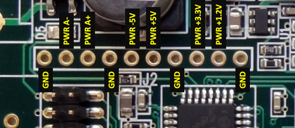
I need power (3.3V), ground and bit clock from the Amanero board:

The 3.3V power supply from the Amanero board can provide up to 50 mA:

The Potato flip flop only consumes a miniscule amount:

Potato Semi flip flop on a SOIC to DIP adapter board. Unfortunately the only pin I could line up with the Amanero board is the bit clock pin to the input of the flip flop.

Made the necessary connections on the backside of the board: power, ground and the Q and Q-bar outputs for the flip flop. Yeah, no ground plane, but better connections would require a custom PCB.

Mounted on the Amanero board, nice fit.


Used 0.1 uF film capacitor bypass close to the 3.3 V power pin (could be closer, but the Vcc and Gnd pins in the chip are diagonally opposite to each other):

The Clock signal for the flip flop can be tapped from R8 or R9. This is the native, low jitter master clock straight from on-board oscillators. One of the concerns is how to switch between the two clocks as both are needed. Fortunately it was reported that both clock lines can be tied together and connected to the clock input of the flip flop.

Apparently only one clock is active at any one time. By looking at the circuit diagram, the clocks have enable lines that are controlled by the CPLD and thus the CPLD can decide which clock should be enabled and which clock disabled. This is a very nice feature as it allows the re-clocking chip to use both frequencies and thus support both sample rate families: 44.1K and 48K.

I think I’ll make the connections to the two clocks like this:

Here is tapping the clock signals: (yes it is an antenna, but it is the shortest distance). The resistors are the smallest I could find in my recycle bin. Any small value should work I used 220 ohm resistors. The board uses 47 ohm resistors on the clock and data lines.


I have both the Q and Q-bar pins available. Right now it is connected to Q. Late I will use the Q-bar output and see what is the effect.

The entire module will be put in a metal case. That is why I had to reposition the OSCON capacitors. This will provide additional protection against EMI.

I think the box needs a logo or something to look “professional” 🙂

RESULTS
Works right away! and sounds pretty good.
I did a quick test on the different sample rates, 44.1, 48, 88.2, 96, 176,4 and 192 and they all work. I will later do my customary unlock measurement…
I must say, this has been a most satisfying mod.
“PROFESSIONAL” MODEL
Here is a much better done mod by bigpandahk [link]:


PRODUCTION MODEL
Here is a board being developed by Acko [link]

Synchronous Reclocking?
Here is an implementation of synchronous reclocking the I2S signal in the Amanero board reported on diyaudio:
After improvement of getting MCLK from XO instead of using standard PIN 6, I tried reclocking the BCK with same MCLK and the improvement is very positive. Right now I tied PIN43/44 on CPLD together, fed MCLK to reclocker and DAC with 2K resistor. The reclocker is 74AUC1G74 D-type flip-flop at 2.5V (power pull from 3.3V with 330ohm in series). Left side is PCM5102 DAC[530]

The basic idea is to:
- Feed the oscillator clock signal directly to the DAC
- Use the oscillator clock signal to drive a flip flop which reclocks the Bit Clock
This reclocking scheme can be done with any USB-I2S where you can tap a low jitter clock signal. Typically these are the ones that derive the clocks from oscillators rather than internally by the FPGA. A good candidate is Lorien’s XMOS-based WAVE IO
WHY RECLOCK?
The goal is to reduce jitter in the I2S signals, including the master clock by leveraging the fact that the jitter added by a flip flop is much less than the jitter added by a CPLD or FPGA.
Even thought the on-board oscillators are low jitter, the signals coming out of the CPLD have a minimum amount of jitter in the order of 100 psec peak to peak. If we take the master clock straight from the oscillator rather than from the CPLD, we don’t have the added jitter by the CPLD. If we also use this clock signal straight from the oscillator and re clock the bit clock, then this new bit clock will also be of lower jitter than the original bit clock coming out of the CPLD.
HOW DOES IT WORK?
“When PRE and CLR are inactive (high), data at the data (D) input meeting the setup time requirements is transferred to the outputs on the positive-going edge of the clock pulse.”
Here is a logic table for a typical flip-flop (this one taken from Potato Semi 74G74 datasheet)

Basically, the flip-flop re-aligns the edges of the bit clock to the edges of the master clock. From the above table, rows 4 and 5, D (data input) is reflected at Q (output) on the rising edge of the CLK (clock). Thus if we use the clock signal directly from the oscillator (low jitter), and feed the bit clock from the CPLD to the D input of the flip flop, it will be “reclocked” resulting in a lower jitter signal at Q (output)
RECLOCK LR CLOCK AND DATA?
Data is read in reference to the bit clock. As long as the minimum timing requirements are met (set up and hold times), a value of 1 will be read as 1 and a value of zero will be read as zero. It is probably safe to assume that systems are designed with sufficient timing margin that even with a more jittery bit clock, there are no digital errors. Therefore, there is no need to reclock the LR clock and the DATA
WHAT ABOUT TIMING?
There are some timing considerations we need to think about with regard to this manner of reclocking. The master clock coming out of the CPLD is synchronized with the other I2S signals (Bit clock, LR clock and Data). In comparison to the clock signal at the oscillator output (oscillator clock), these signals have a certain amount of propagation delay just for the fact that they have gone through the CPLD device. I am not exactly sure how much is the propagation on the output signals, but based on the CPLD datasheet, it may be in the order of 10 (or 10s) nano-seconds.
When the bit clock is reclocked with the oscillator clock, the new reclocked bit clock will be further delayed because it would have likely missed the rising edge of the oscillator clock (the signals out of the CPLD are delayed by the propagation delay) and would have to wait for the next rising edge of the clock signal.
How much is the bit clock delayed?
As discussed, the flip flop aligns the new bit clock to the rising edge of the oscillator clock. The oscillator clock is ahead (timing wise) of the master clock to which the bit clock is synchronized. The bit clock would have likely missed the rising edge of the oscillator clock and needs to wait for the next rising edge of the oscillator clock. The resulting new bit clock is thus delayed ONE PERIOD time of the oscillator clock. (It could be half a clock period depending how the signals are synchronized to the master clock: rising or falling clock edge)
One period for a 22.5792 MHz clock is 44 nsec. The bit clock for 44.1 KHz material is 354 nsec. The potential maximum delay of the new bit clock is a small percentage of the width of the bit clock which in this case is 44/354=12%. There should be no problems as also reported working by the poster above.
However, for higher sample frequencies, the delay becomes a larger percentage of the bit clock width. If we look at 172K material, the bit clock period is 88 nsec and the delay in the new reclocked bit clock is 50%. Perhaps this will still work. Increasing the sample rate further, say 352K sample rate, the delay is the same as the width of the bit clock. This will result in completely missing the first bit of the data signal.
CANDIDATE DEVICES
- The Experimenter above uses 74AUC1G74 D-type flip-flop (operates at 1.8v)
- A better fit with 3.3V operation is the SN74AUP1G74
- Also recommended in the forums with even wider operating voltage: 74VHC74
- This flip flop is used in Ian’s FIFO Clock board (3.3v operation): 74AUP1G79
- Potato Semiconductor 74 Series Logic: PO74G74A. Extremely fast and very low propagation delay.
Some would argue that because the Potato Semi device is the fastest device, the added jitter is smallest. This would make sense. The technology used by Potato Semi in their devices are based on noise reduction which helps reduce jitter.
WHO IS POTATO SEMICONDUCTOR?

Based on the funky name, company log0 and the bare design of their website, Potato Semi seems a company of dubious reputation. However this is a company that have invented some cool technology. Here is the invention if you are interested in reading patents [link].
According to the press:
Potato Semiconductor, a leading IC design company focusing on the high speed CMOS I/O field, has successfully applied its innovative technology to 74 series logic ICs. Using advanced technology, this new generation of 74 series logic ICs features high performance, high frequency and low noise. The running speed can be 5 to 7 times faster than existing 74 series ICs which continues the prevailing trend in electronics design — high speed and high performance.
But the strongest vote of confidence comes form Ian’s FIFO reclocker. He has experimented with Potato Semi chips and has selected it for his latest clock board [link].
The chip can be purchased direct through eBay for $3. Not cheap in comparison with standard logic chips which cost in the order of $0.50. But for a few bucks you can (theoretically) drastically reduce the output jitter of the Amanero board (or other interface with similar design)
INTERFACING TO BUFFALO DAC
The synchronous reclocking approach described here seems ideal for interfacing with the Sabre DACs for the following two reasons:
- The oscillator frequency of Amanero (22.5792 MHz and 24.576 MHz) is below what the Buffalo DAC considers “normal” which is higher than 40 MHz. So the best way is to operate the DAC in its normal asynchronous mode, taking advantage of the DAC’s local oscillator
- The DAC locks to the bit clock, therefore it is desirable to generate a low jitter bit clock with this method of using a flip flop driven by a low jitter oscillator clock
PROS
- Reduce jitter to the absolute minimum possible with the board
- Easy to do, low cost
CONS
- May not work for higher sample frequencies
This would be a very nice and interesting (and very cheap) mod. Definitely worth trying it out. I’ve already ordered some Potato Semi flip flops.
REFERENCES
Potato Semiconductor: http://www.potatosemi.com/
TI Logic Guide: http://www.ti.com/lit/sg/scyt129e/scyt129e.pdf
BBB DAC DEVELOPMENTS
As many know, the BeagleBone Black I2S audio implementation is in a way superior to the I2S audio implementation of the Raspberry Pi primarily because the audio clocks can be derived from the on-board 24.576MHz clock and also through off board oscillators through an I/O pin. It its current implementation, the BBB supports the 48KHz family of sample rates with the on-board oscillator and can support the 44.1KHz family of sample rates with an off-board oscillator.
The current method of generating the clocks for digital audio in the Raspberry Pi are far from perfect. The best clocks are obtained by integer division of the on-board 19.2 MHz clock and works for 48K and 96K sample rates and only if the DAC can accept 40fs or 80fs. For anything else, the clocks are derived from the 500MHz PLL through fractional division as explained above. It has been reported that the 500MHz clock itself is derived from the on-board 19.2MHz clock through a clock multiplier.
Even with a “superior” audio clock implementation, I2S DAC development for the BBB has been painfully lagging that of the Raspberry Pi (so painful that there are no products shipping). The reason is because that there is a lot, lot more community development in the Pi than the Beagle. The RPi has just shipped its 5 millionth device [link] whereas the BBB has only shipped about 220K devices [link].
No longer.
TWISTEDPAIR AUDIO
Twistedpair Audio has been busy designing and testing external components to allow the BBB access to lower jitter off-board oscillators and data reclocking for ultimate I2S signal fidelity. These boards are almost ready for general sale [link]
Update 3/26/15: they are available for sale [link], and pretty reasonably priced given the components. (The store says “introductory pricing” though)
The mockup photo below shows (from right to left) BBB, “Hermes”, “Cronus”, and Buffalo III DAC. The board on the top is the Hermes board for the Amanero interface. With Hermes-Cronus, Amanero can use better off-board clocks if so desired.

These links explain the functionality of these boards [link], [link]
- BBB as the source of I2S/DSD digital audio, it needs external clocks in order to support all sample rates
- Hermes as the two-way signal isolator (clock signal into BBB, audio data signals out of BBB, and I2C in-out) and I2S/DSD switch. Hermes also has connections for a volume pot, push buttons, etc. that interfaces to I/O pins in the BBB -more details below (priced at $40 or $16 for the board only)
- Cronus is the clock board which can accommodate two clocks: one for 44.1KHz sample rate family and one for 48kHz sample rate family. Cronus also provides data realigning of the I2S signals (as opposed to FIFO reclocking) – more details below. (Priced at $50)
- Clock modules. The clock modules are available separately from the Cronus board with a choice of frequencies and are priced at $35 each. You need two.
- Total is $160 for Hermes+Cronus+Clocks. You don’t really need the Hermes if all you are interested in are the clocks, so the minimum investment is $120
Here is a photo of the updated Hermes board (the interface/isolator board between BBB and Cronus)

- Provides isolation for audio signals with 1 -8 channels of PCM – 1 – 4 channels of DSD output
- Provides I2C isolation
- SPDIF output is possible.
- Lots of headers: for Switches/Rotary encoder and drivers for indicator LEDs; USART header, ADC header for analog control; headers for external power/reset switches.
- Prototyping area (for fun!)
- Provision for backup battery to protect the BBB on shutdown by providing a soft shutdown(self regulating battery not included in the kit – but very easy/cheap to obtain).
Here is a photo of the updated Cronus

- Ultra low noise low impedance power supply for clocks (adm7150)
- A clock selection multiplexer to switch between 44.1 and 48Khz time bases (this means the source must output a clock selection signal). The clocks are isolated from each-other and the rest of the circuit by utilizing L/C filtering
- A selectable/bypassable ultra low phase noise clock divider to supply 1:2 or 1:4 clocks to a source
- A synchronous reclocker that re-clocks the audio from the source back to the master clock. This brings all signals back into alignment with the actual master clock regardless of source jitter. Uses Potato Semi flip-flops. To learn more, here is my crude attempt at reclocking [link]
- SMA and uFL connectors for external clock signals (both in or out), uFL connectors for PCM/DSD output.
IQAUDIO
IQAudio’s main products to date are audio boards for the Raspberry Pi. As I wrote here [link] their DAC board is one of my favorite for the Raspberry Pi. The DAC boards for the RPi are also very popular, often sold out at the Tindie store [link]
The IQAudio BBB DAC is aimed at a full I2S DAC solution for the Beagle. A photo of a prototype is shown below.As can be seen in the photo, there are no external clocks that can be fed to the BBB. Normally a DAC operates in Slave Mode. The DAC locks to the master clock or bit clock of the source and receives the data from the source device. In the IQAudio solution, the DAC instead is running in Master mode. The DAC generates the appropriate bit-clock frequencies in accordance to the sample rate of the track being played and it “pulls” the data from the BBB. You may follow its development here [link].
According the manufacturer, the board will be available in May at a target price of $45-$60. Please send your queries and comments to IQaudio at Gordon@iqaudio.com.
Notice also the I2S headers. Possibly you can use this board and tap the I2S signals and use them for another DAC board.

Comparing with the RPi DAC which is shown below, it seems the BBB DAC uses almost the same components. The innovations are in software: drivers in the BBB side and firmware to setup and control the DAC chip.

There is also an advantage of buying a product from iQAudio (and other similar companies such as HifiBerry) in that they invest in software development (drivers) and provide many ready-to-run software distributions for your embedded computer.
ACKO SUPERCAPE
Acko is also planning to release a BBB cape that is derived from their current clock/isolator board which is already a working solution for the BBB. A nice photo from this post [1828]:

The “supercape” adds battery management to the capabilities of the current clock board in an integrated package. It will provide:
- UPS kicks in when external power is removed. On-board PWR_MON will continue to power the BBB (~1hr) or options to safely shutdown BBB immediately. Same shutdown action if battery level goes below operational level [1088]
- High Speed Galvanic Isolation with -Synchronous or Asynchronous re-clocking.capability
- Ultra-low jitter Dual Synchronous Audio Clock (98.304MHz/90.3168MHz or 49.152MHz/45.1584MHz options) – Master Clock
- All buffered outputs with high drive capability
- GHz rated switching components
The following diagrams show the work-in-progress for this cape, starting with adding a USP and interface for the BBB and the clock board to the current configuration of a fully integrated cape.
From: [1088]

[1332]

From [1587]:

SOEKRIS dam1021 DAC
The Soekris R2R DAC supports the BBB in synchronous slave mode by providing the required master clock frequency as selected by the BBB. BBB is in master mode, but the DAC provides the clock
- I2S MCLK OUT pin: Master clock output: 45.1584 and 49.152 Mhz (which can also be divided)
- I2S FSEL IN pin: Input signal at this pin selects between 45.1584 MHz and 49.152 MHz master clock output
It works in a similar fashion as the TwistedPair and Acko solutions but it has been incorporated into the DAC.
I have yet to experiment with it myself but has been reported to work: [link]
The Soekris R-2R DAC: Technical Details


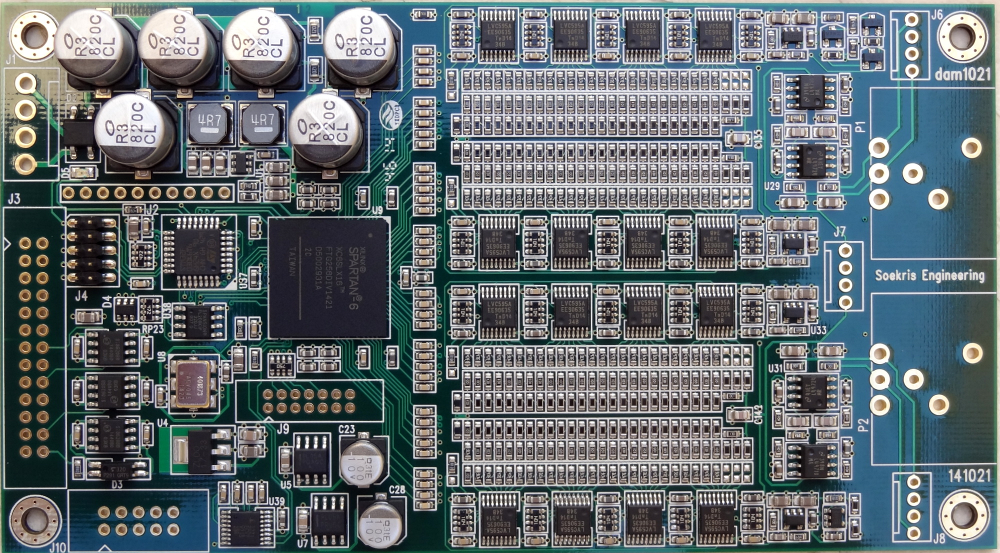
The Soekris R2R DAC is finally out, officially named
The Soekris dam1021 Sign Magnitude R-2R DAC
I will be collecting useful information here and in other posts because as the thread at diyaudio gets longer, it would be difficult to find things…
USERS GUIDE: [link]
INITIAL FEATURES
The initial release (“v1) of the firmware together enables the following features:
- I2S input up to 384KHz sample rate (tested to 192KHz)
- SPDIF input up to 192KHz (tested to 96KHz)
- Automatic De-emphasis for 44.1KHz material
- Built-in set of simple FIR filters for all sample rates
- Digital volume control through simple potentiometer
- Automatic input selection
- Data reclocking: s/w PLL with 0.02 Hz low pass filter
- S/W interface (serial interface) allows:
- Volume control (e.g. with Arduino and RS232 interface)
- Input selection (e.g. with Arduino and RS232 interface)
- Loadable FIR filters including bypass filter for NOS support (s/w utility included)
- Firmware update/upgrade
Upcoming features (through user-performed firmware upgrade)
- DSD support
- Filter cascading for digital crossover
- Filter cascading for balanced use
- Master clock output
- 4 FIR1 filters for each sample rate selectable through the serial port with a default selection (#2)
- Linear Phase
- Medium, optimized mix between Linear Phase and Minimum Phase
- Soft, mostly Minimum Phase but not that good alias rejection
- No filter, also called non oversampling, no alias rejection
- Improved response for FIR2 filter which will be modified to be pretty soft….
- Enabled TTL-level serial port on the isolated side (3.3v)
Rather than incremental updates, Soren is planning a big update [link]
USERS GUIDE: [link]
AUDIO OUTPUT
Ref: [link]
The dam1021 DAC “raw” audio output is DC-coupled. The signal out of the resistor ladder passes through a low pass RC filter consisting of a 1200 pf ceramic NP0 type (“audio” grade), and the -3db point is at ~250 Khz (different values have been reported but at this cutoff, it doesn’t really matter to the audio frequencies).
The specs of the raw output are:
- 0V offset (no need for DC blocking capacitor)
- Output level: 1.4V RMS
- Output impedance: 625 ohms, purely resistive.
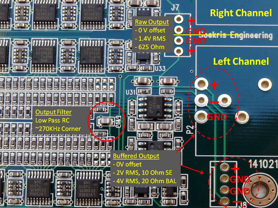
The raw output is available for single-ended connection. It is also routed to a single-ended to balanced output buffer according to the following schematic:

- LME49710: High Performance, High Fidelity Audio Operational Amplifier. Data sheet: [link]
- LME49724HighPerformance, High Fidelity, Fully-Differential Audio Operational Amplifier. Data sheet: [link]
The buffered output can be used single-ended or balanced. It can drive high impedance headphones directly.
The specifications for the buffered output are:
- Output level: 2V RMS SE, 4V RMS BAL. The output of the Differential Opamp can be used either single-ended (SE) or differential (BAL)
- Output Impedance: 10 ohm SE, 20 ohm BAL
- Output DC offset: per datasheet p.14: “The VOCM pin should be connected to ground when the desired output common-mode voltage is ground reference”. Thus based on the schematic, the DC offset = 0
Update:
Staring with Rev4 of the board, the buffered output implementation has been replaced with OPA1602 dual OpAmps: [link], due to end of life of the products that originated with National Semiconductors [link][link]. Likely the last of the engineers from the “analog golden era” have retired…
POWER SECTION
Reference: [link], [link], [link]
Main Power Section

- Designed to be powered by a single dual 7-8V AC, 5W transformer (since it has has a bridge rectifier installed)
- Can also take an external +/- 7-15V DC supply. (See section above on power supply requirements for further details)
- Actual power consumption has been measured to be 2.4W.
- Filter capacitors are Nichicon 820uF 16V CL series [link]
- Negative voltage is required for the output opamps and other parts of the circuit [link]
- A DC-DC converter (switch mode) provides the 1.2V for the FPGA core. Every other supply is low noise linear [link]
- “The LME output buffers are powered via an additional large RC filter after the main capacitors, no active regulators. With a typical PSRR of 125 db I didn’t worry much about 100/120 hz ripple, only worried about higher frequency noise on the power rails….”
Input Voltage [901]
- DC: +/- 7 to +/-15V DC; preferable 9-12V DC
- AC: 2x 7-8V AC
- Power goes though a diode bridge so polarity doesn’t matter. Connector is MTA156 type.
Maximum and Minimum Input Voltage [848]
- Upper limit of 16.5V, based on capacitor voltage and also to limit loss in linear regulators.
- Lower limit of 7.5V, based on loss though diode bridge and 5V linear regulators.
- Taking into account line voltage tolerance and transformer no/low load voltage, this results in the 7-8V AC requirement for transformers.
Power Consumption [1130]
- Positive Rail: .18A, 10V
- Negative Rail: 0.06A, 10V
- Total: 2.4W
- The positive supply draw about 3 times as much current as the negative; the current is almost independent of input voltage.
1.2V Supply
The DC-DC regulators is the TI TPS562209 [link]
Here is the reference circuit taken from the datasheet:

3.3V Supply
A 3.3V LDO Powers the Clock [link]

It is a pretty hefty regulator. And it seems the only 3.3v regulator on the board. It must also supply 3.3V to:
- 3.3V need of the FPGA
- Clean side of signal isolators
- SPDIF LVDS receivers
- Microprocessor
- Flash memory
- Other components (like the shift registers?)
Good thing it is implemented next to the clock of all places.
Reference Voltage Supply
The most critical supply is the +/- 4V reference for the resistor ladder. This is generated by a “two step, first to +- 5V (by linear regulators), then to +-4V by precision low noise medium current opamps”; “-4V reference is sent though an inverter with 0.01% resistors generating the +4 reference”. The references are further “filtered and buffered for each rail and channel”.
Linear Regulator for +/- 5V
The 8L05A and 9L05A are +5 and -5 Linear regulators [link]. Input to these regulators are the +/- rails (which could be 7 to 15V regulated or unregulated) . The outputs are filterd by 100uF capacitors.


Power Rails Connector/Header [1144]
J2 is a connector to all the power rails, for testing or for supplying (limited) power to other things. The 1.2V can be used to bias the LVDS for Coax SPDIF input (see users guide)
DIGITAL FILTERS [1285]
Original (current) digital filters:
- FIR1, upsampling from incoming sample rate to 352/384 KHz in one step, with different filter length based on incoming sample rate. All FIR1 filters are basic Parks-McClellan “brick-wall” types, designed with http://t-filter.appspot.com/fir/index.html, but still shorter than your regular DAC.
- FIR1 is automatically bypassed if feeding 352/384 KHz data.
- IIR, bank of 15 bi-quads operating at 352/384 KHz, with one used for the CD de-emphasis filter, none otherwise used for the basic DAC.
- FIR2, upsampling from 352/384 KHzto 2.8/3.1 MHz, reasonable short and soft but still using same design as FIR1.
- All filters are using 32 bit coefficients, with up to 67 bit MAC accumulator.
I’m not a believer in no filters (non oversampling), but also don’t like the sharp “brick-wall” filter types with the pre-ringing. The goal is to work towards filter types that remove just enough to not cause problems with aliasing. It’s pretty easy with higher sampling rates, but is long and hard work and listening tests with 44.1 KHz, which still are the sample rate mostly used….
Further details on the filters [link]
FIR1
FIR1 is operating at 352.8K/384K (output frequency of the filter and this is set in hardware [link]) and each filter can have up to:
- 1016 tabs at 44.1K/48K input sample rate
- 508 tabs at 88.2K/96K input sample rate
- 252 tabs at 176.4K/192K input sample rate
- 124 tabs at 352.8K/384K input sample rate, but normally bypassed
This also means that:
- 44.1K/48K input sample rate, the oversampling filter must be 8X
- 88.2K/96K input sample rate, the oversampling filter must be 4X
- 176.4K/192K input sample rate, the oversampling filter must be 2X
- 352.8K/384K input sample rate, , the oversampling filter must be 1X, but normally bypassed
All upsampling is done by zero insertion, therefore gain needs to be set to match oversampling rate.
- For 44.1KHz/48KHz sample rate the upsampling is 8X, thus the gain should be 8
- For 88.2KHz/96KHz sample rate the upsampling is 4X, thus the gain should be 4
- For 176.4KHz/192KHz sample rate the upsampling is 2X, thus the gain should be 2
- For 352.8KHz/384KHz sample rate the upsampling is 1X, thus the gain should be 1 (But this filter is normally bypassed
Headroom for clipping prevention due to oversampling and the required applied gain [link]
The dam1021 have 2-4 bit of headroom though the digital filters, all the way until the volume control. So any clipping would be because of incorrect filters.
Why not one step oversampling to 2.8/3.1 MHz? [1557]
Not that practical, would require > 3000 taps. In addition, the intermediate frequency is good to have for the CD de-emphasis and crossover filters.
352K/384K is as a good compromise for the intermediate rate, so there is space for enough IIR filters for crossover use and room correction. If you go up you get less IIR filters. # filters = 45M/49M divided with intermediate rate divided with 8 = 16.
FIR2
FIR2 is operating at 2.822M/3.072M and can have up to 120 tabs, with input sample rates 352.8K/383K. The FIR2 filter don’t require much, I’m looking into doing a bessel or butterworth type filter there.
dam1021 FPGA fixed point format [link]
The filter file 1021filt.txt [http://www.soekris.dk/1021filt.skr]
There can be multiple of each filters in the 1021filt.txt filter file (part of the filter tools), but at least one (filter) needs to be there for each input sample rate. Currently just the first one for a given sample rate is used, in later firmware releases you will be able to choose between different filters
Filter tools
Filter tools and documentation will be shortly available for users to upload custom filters to the FPGA. The tools are already available here: [link]
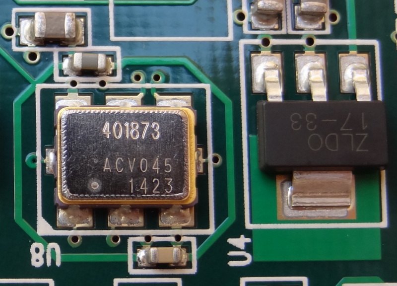
CLOCK SECTION
The clock in the dam1021 DAC is the Si514. This the lower grade of programmable clocks from Silicon Labs (.8 psec RMS jitter) [link], and according to Soren, it is well matched to the system as a whole. It is also used instead of the Si570 because of lower power consumption.

Master Clock Output Pin [848]
- I2S MCLK OUT pin: Master clock output: 45.1584 and 49.152 Mhz (which can also be divided)
- I2S FSEL IN pin: Selects between 45.1584 MHz and 49.152 MHz
Same master clock output is also used when connecting multiple DAC’s, for example for digital crossover applications.
Here is a comparison jitter measurement between the Soekris DAC and other DACs [link], [link], [link]

Jitter reduction is accomplished with signal reclocking through a short FIFO. The data is received into a configurable FIFO and then it is reclocked with a lower jitter clock, eliminating most of the incoming jitter.
Further details [link]
The details of my clocking/FIFO:
Ian’s FIFO use a fixed clock, and therefore use a large buffer to take up the difference between incoming and outgoing clock. That add a large delay, which doesn’t matter for simple audio applications but are undesirable in a number of applications, like home theater or live music.
I use a much shorter FIFO, selectable down to 1 mS, and instead adjust the outgoing clock to match the incoming clock frequency as needed, being I2S or SPDIF. The Si514 oscillator used is very low jitter and digitally programmable with a resolution of 0.026 ppb (parts per billion, not million…). It also have the feature that reprogramming inside +-1000 ppm is glitchless, ie the clock adjust very nicely to small changes.
SERIAL INTERFACE
The DAC has two serial interface:
- Standard RS232 serial interface
- TTL level Isolated Serial interface (requires firmware > 0.9)
The RS232 interface is provided by the Intersil 3221ECVZ chip [link]
The Intersil ICL3221E devices are 3.0V to 5.5V powered RS-232 transmitters/receivers which meet ElA/TIA-232 and V.28/V.24 specifications. Additionally, they provide ±15kV ESD protection on transmitter outputs and receiver inputs (RS-232 pins).
Valid RS232 levels are >+2.7V and <-2.7V according to the datasheet. Strictly speaking is > +2.4V and < -2.4V but under +/- 2.7 V it may trigger the auto power-down.
Notice that pins 9 and 11 are the TTL level serial lines to/from the FPGA. The chip convert those signals to RS232 compatible levels and provide the robustness of the RS232 standard.


Automatic power down
The chip has an automatic power-down function for noise reduction. When no valid RS-232 voltages are sensed on the receiver input for 30µs, the charge pump and transmitters power-down, thereby reducing supply current to 1µA.
The ICL32xxE powers back up whenever it detects a valid RS-232 voltage level on the receiver input. This automatic power-down feature provides additional system power savings without changes to the existing operating system.
The chip is a drop in Replacements for MAX3221E, MAX3222E, MAX3223E, MAX3232E, MAX3241E, MAX3243E, SP3243E, meaning it should be fully compatible with USB interfaces implemented with those chips.
MY OTHER POSTS ON THIS DAC
| TITLE | SUBJECT |
LINK |
DESCRIPTION |
| Soekris dam 1021 R-2R DAC ILLUSTRATED GUIDE | Users Manual | [link] | Users manual for the Soekris DAC. |
| Soekris dam1021 Build | Build Guide | [link] | Details of my initial build of the Soekris DAC. |
| dam1021 R-2R DAC MODs | Mods | [link] | Mods I have performed on the DAC build. |
| dam1021 R2R More Mods | Mods | [link] | Later mods on the DAC build. |
| Digital Filters for Soekris R2R DAC | Digital Filters | [link] | Extensive list of DIY filters from the diyaudio filter brewing forum thread. |
| R2R Benchmark Filters (for now) | Digital Filters | [link] | Latest set of filters developed and shared in the diyaudio filter brewing forum thread. The best filters of the bunch. |
| R-2R DAC For The REST of US | Technical Details | [link] | Introductory post describing the innovations and capabilities implemented in this DAC. |
| The Soekris R-2R DAC: Technical Details | Technical Details | [link] | Additional technical details of the Soekris DAC that were not covered in the post above and collected after I had the DAC on my hands. |
Raspberry Pi B+ Digital Audio
I2S AUDIO
Although the Raspberry Pi has built-in analog audio output, the interest here is in digital audio output in particular I2S output signals for direct connection to digital to analog converters. I explored a bit the digital audio capabilities of the Raspberry Pi a while ago [link]. Here is an update with more accurate information.
The digital audio capabilities of the Raspberry Pi B+ have not changed from previous versions. The I2S audio is supported by the Broadcom BCM2835 [link] peripheral SoC chip. The datasheet shows that the PCM audio interface consist of 4 signals, notice that there is no Master Clock signal:
- PCM_CLK – bit clock.
- PCM_FS – frame sync signal. Frames can be up to 32 bit wide
- PCM_DIN – serial data input.
- PCM_DOUT – serial data output.
In addition, for more advanced configurations, the device can be configured as master or slave: “the direction of the PCM_CLK and PCM_FS signals can be individually selected, allowing the interface to act as a master or slave device”. In normal operation, it is configured as a master device.

In the Raspberry Pi B+, The I2S output are assigned to the following pins:

EXTERNAL CLOCK
The audio frequencies (the PCM _MCLK) are supposedly generated by the use of a discrete 0n-board 19.2 MHz crystal. Unlike the BeagleBone Black, where there are facilities (pins) to feed an external master clock.

The frequency that is generated at any of the I/O pins, say the bit clock, is obtained by dividing the source clock (19.2 MHz oscillator) by configuring a clock division register with an integer part and a fractional part as indicated by the datasheet excerpt shown below:

The Datasheet indicates that the clocks are generated by “noise-shaping MASH dividers” which are fractional dividers. It also says that “The fractional dividers operates by periodically dropping source clock pulses”. I believe this post has an example on how this is actually implemented [link].
The way that a 3.25x clock divider is implemented is by dividing by 3x for some periods and 4x for other periods, with the average being 3.25x. In this case the repeating pattern will be (3, 3, 3, 4). That is shown in the following scope capture. Note that the first three periods are divided by 3 and then the next is divided by 4.The way this is implemented in the device is to divide by the smaller divider and then extend the high pulse width by one clock cycle periodically.

We can find the integer divider and fractional divider based on MASH 1 (see above) and determine what is the maximum and minimum output frequency:
- Source clock: 19,200,000 Hz
- Sample rate: 44,100 Hz; bit clock (64fs)=2,822,400 Hz
- Actual divisor: 6.8027. Integer part=6
- Fractional divisor: =0.8027×1024=822 (round off)
- Maximum frequency: 19,200,000/6=3,200,000 Hz (50 KHz sample rate)
- Minimum frequency: 19,200,000/7=2,742,857 Hz (42.9 KHz sample rate)
- Average frequency: 19,200,000/(6+(822/1024))=2,822,394 Hz (44.1 KHz sample rate)
Well, aiming at 44.1KHz sample rate frequency and getting a frequency variation from 42.9 KHz to 50KHz, this can’t really work for digital audio. Clearly there has to be a better way to generate these clock frequencies.
GENERATION OF DIGITAL AUDIO FREQUENCY CLOCKS
Much of the credit for enabling I2S output in the RPi (and the proper generation of clock frequencies) is due to the discussion in the Raspberry Pi forums [link] and work of Florian Meier in his master thesis “Low-Latency Audio over IP on Embedded Systems” [link] who subsequently developed the basic “ALSA SoC I2S Audio Layer for Broadcom BCM2708 SoC” audio kernel driver [link]
There it is explained that in order to get good clocks, one has to use integer division but with a 19.2 MHz clock, it is impossible to arrive at 32fs or 64fs bitclocks (e.g. 64x48KHz=3.072 MHz). Therefore other internal clocks must be used.
According to this post [link] the clocks sources are:
0     0 Hz     Ground
1     19.2 MHz oscillator
2     0 Hz     testdebug0
3     0 Hz     testdebug1
4     0 Hz     PLLA
5     1000 MHz PLLC (changes with overclock settings)
6     500 MHz  PLLD
7     216 MHz  HDMI auxiliary
8-15  0 Hz     Ground
The logical choices are the external 19.2MHz and the highest stable frequency clock which is the 500 MHz clock (highest frequency generates a more accurate clock after fractional clock division)
The author presents two solutions:
- Use the 19.2 MHz oscillator with integer division for DACs that do not require a specific ratio of bit clock to frame sync (e.g. 32fs for 16 bit data) as long as there are at most enough bit clock cycles within a frame sync cycle to contain the desired word length
- Use the 500 MHz internal PLL with fractional division for DACs that do require a specific ratio of bit clock to frame synch (e.g 32fs or 64fs)
The first solution says that it is possible to use, say 40fs, to sent 16 bit samples (16bitx2=32bit per frame) because you can transfer all 32 bits in a 40 bit frame. If you can use 40fs for the bitclock, then 40x48KHz= 1.920 MHz which is 19.2 MHz/10. The following excerpt from the thesis explains these two approaches:

We notice that integer division of the external 19.2 MHz clock only works for 48KHz and 96 KHz and for DACs that can operate at 40fs (80fs if we want to pass 32×2 bits per frame). The current version of the code is using 50fs and 100fs which also works.
For the 44.1KHz sample rate or for bitclock requiring 32fs or 64fs, then the first solution with fractional division is used on the 500 MHz PLLD clock
WHY 19.2 MHz CLOCK?
The fact that no clean clocks can be generated in the digital audio frequency range, tells us that this oscillator was not really meant to be used for digital audio. Now why did the designers of RPi use a 19.2 MHz clock?
I have searched extensively and cannot find a “reason” for the 19.2 MHz frequency. If it were digital audio, a more logical selection would have been 24.576 MHz in order to cleanly support 64fs 48KHz sample rate (like the BeagleBone Black).
A better reason is to use this clock for the on-board PWM audio. One can easily generate a 48KHz carrier frequency (19.2MHz/40) and a resolution of 16 bit would require a frequency of approx 64 KHz (19.2MHz/30). In actually, it has been reported that the resolution is in the neighborhood of 11 bit or 2048 levels which can be obtained by dividing 19.2MHz by a factor of 9375.
SLAVING THE RPi
A better solution is to configure RPi as a slave device and the DAC as a master device.
The DAC can provides a much more accurate clock to the RPi by feeding the Bitclock. I don’t think is being done by the current crop of DACs (the ones based on the PCM5122) but the capability is there for both in the RPi (“clock slave mode” and “frame synch slave mode”) and the PCM5122 as shown in the following excerpt from the datasheet:

Here is what is required to set the DAC in Master Mode, say for example the PCM5122.
- RPi detects the sample rate of the clicked-to-play track.
- RPi has a way to indicate the sample rate (for example using GPIO pins).
- Microcontroller reads sample rate.
- Microcontroller programs the appropriate frequency by generating an appropriate master frequency from the PLL and setting the appropriate divider to generate the bitclock.
Other considerations:
- Timing of the different events. For example, wait until the microcontroller programs the DAC to the appropriate clock frequency before staring the data stream (DMA) in the RPi.
- Selection of external clock. For example use a single frequency clock, say a multiple of 44.1KHz in order to take advantage of integer divider only when dealing with frequencies multiple fo 44.1KHz.
COMPARISON WITH OTHER DEVICES
Here is the previous comparison table with some updated observations (italics)
| Parameter | Rasberry Pi |
BeagleBone Black |
Comments |
| Native I2S support | Yes | Yes | Both platforms can support I2S output, Custom drivers have been developed by the audio community |
| I2S Sample Rate limitation | Up to 192KHz (because the on-board clock is 19.2MHz) | Only 48KHz family (because the on-board clock is 24.576MHz and integer clock dividers) | BBB supports 48KHz, 96KHz, 192KHz and 384KHz. RPi supports 44.1KHz, 48KHz, 88.2KHz, 96KHz, 176.4KHz and 192KHz (in theory). RPi uses “fractional clock dividers” to generate the 44.1KHz sample rate family as explained above |
| Support for USB DAC | Yes (LAN9512 chip [link]) | Yes (Built-in in the main processor) | USB in the RPi goes through a built-in HUB and it is shared with the LAN controller within the USB/LAN chip. USB in the BBB is natively supported by the main processor; LAN has a separate chip |
| Support for external, low jitter clocks | Not possible unless you replace the on board oscillator and modify the driver | Yes with custom boards and custom s/w: [link] | The master clock in BBB may be provided externally by disabling the on-board audio-freq clock.The Master clock in the RPi seems internally generated and there is no I/O pin to feed an external master clock |
| Master clock output | No | Yes (from on-board clock) | The Master clock in BBB is provided by the on-board 24.576MHz and fixed at this frequency and can be directly accessed from the outside. The Master clock of RPi seems internally generated but un-accessible from the outside. Without Master Clock, you can only use DACs that can operate asynchronously without a Master Clock input such as the ESS DACs or DACs that can operate with the master clock = bit clock |
| Built-in rechargeable battery operation | No | Yes [link]. Maybe | Rechargeable Battery operation in BBB would disable the 5V supply to the USB. Thus for USB operation, where the USB adapter takes the power from USB, BBB must be powered with 5V DC |
| Built-in Storage | No. But the new model has plenty of USB ports for USB memory sticks | 2 GB eMMC Flash | BBB can boot from the internal storage freeing the SD card for music storage. RPi requires that the OS be stored in the SD card (although it may be possible to also store music in the SD card) |
| Looks | The latest model looks Good | Good | 🙂 |
| Audio H/W and S/W community support | Large | Small | |
| Price | $35 | $55 |
Here is a summary of the phase noise measurements from this post [link]:

Observations
- The ESS9023 implements a “jitter eliminator” (asynchronous sample rate converter) but cannot eliminate all the jitter
- The clocks on the embedded boards have a lot of jitter. It also makes sense that the BBB has better measurement than the RPi. In the BBB, the 48KHz sample rate frequency is derived by integer division of the external clock. In the RPi, the 44.1KHz sample rate frequency is derived from the 500MHz clock which is derived from the external clock as explained above
- The “lowly” CD player is still a pretty good playback device in terms of jitter
- I would guess (and only a guess since the author does not identify these interfaces) USB-I2S-2 is an XMOS-based device based on how the clocks are generated and that USB-I2S-1 is a device based on an FPGA or CPLD using two external audio frequency clocks (where straight integer division is used)
SUMMARY
The current method of generating the clocks for digital audio in the RPi are far from perfect. The best clocks are obtained by integer division of the external clock and works for 48K and 96K sample rates and only if the DAC can accept 40fs or 80fs. For anything else, the clocks are derived from the 500MHz PLL through fractional division as explained above. It has been reported that the 500MHz clock itself is derived from the 19.2MHz external clock through a clock multiplier.
However imperfect as these clocks might be, there are a good number of DAC boards that have been developed and reported to work well with the RP1. As these products are being developed by audio fanatics, we can expect continuous improvements and enhanced approaches to better clock generation such as external reclocking and slave configurations.
For additional info, you can check the Raspberry Pi I2S discussion thread here: [link]
R-2R DAC For The REST of US
A MOST INTERESTING DIY PROJECT IN A LONG TIME
A Discrete R-2R Sign Magnitude 24 bit 384 Khz DAC [link].
The DAC Module includes all local power supplies, a programmable low jitter clock, Micro-controller and balanced output buffer. It is implemented on a 4-layer PCB. The board size is 3.2″ x 5.8″ (81 x 147 mm).
As the industry migrated from R2R topologies to Sigma-Delta in their quest for higher bit-depth, higher performance (and cost management), present implementations of R2R DACs are pretty much hand-crafted commanding a high premium.
As the author states:
“I believe that the sound quality will be the absolute best, better than any Delta Sigma DAC, in class with discrete DAC’s from totaldac and msb technology. And for way way less cost :-)”
For the rest of us with limited resources wanting to experience a ladder DAC, this is the DAC to have.
An excerpt from the PCM1704 [link] datasheet expunds the good points of a ladder DAC:
Digital audio systems have traditionally used laser-trimmed, current-source DACs in order to achieve sufficient accuracy.
However, even the best of these suffer from potential low-level non-linearity due to errors in the major carry bipolar zero transition. Current systems have turned to oversampling data converters, such as the popular delta-sigma architectures, to correct the linearity problems. This is done, however, at the expense of signal-to-noise performance, and the noise shaping techniques utilized by these converters creates a considerable amount of out-of-band noise. If the outputs are not properly filtered, dynamic performance of the overall system will be adversely effected.
The PCM1704 employs an innovative architecture which combines the advantages of traditional DACs (e.g., excellent full-scale performance, high signal-to-noise ratio, and ease of use) with superior low-level performance.
Granted, that was circa 1999. Since then the Sigma-Delta camp has made great strides. Even so, R2R DACs have not lost their appeal as witnessed by the interest in this project and the current commercial offerings.
TARGET PRICE
The DAC module is not yet available for sale. The target price is US$240 with 0.02% resistors. This is a steal considering how much other R2R implementations cost.
ADVANCING THE STATE OF THE ART
The last commercially available R2R DAC chips were the PCM1704 [link] and the AD1865 [link]. They have been out of production for a long time but still available for purchase for example here [link] and here [link].
Here is a table comparing selected performance numbers and features as described in the data sheets and by the author in the diyaudio discussion thread.
- The PCM1704 is typically used withe a companion chip, the DF1704 [link].
- The AD1865 is also used with a companion filter chip such as the Sony CXD1244S [cxd1244s]
| Parameter | Seokris R2R |
PCM1704+DF1704 | AD1865+Digital Filter |
| Max Input Sample Size | 24bit | 24bit | 18bit |
| Max Input Sample Rate | 382KHz | 96KHz | 44KHz |
| Max Resolution | 28bit (1) | 24bit | 18bit |
| Inputs (2) | 1x Isolated I2S, 3x SPDIF/TOSLINK/AES/EBU [link]; future DSD upgrade | Serial only (DF1704: LJ, I2S) | Serial only through the digital filter chip |
| S/W Interface | Serial (Not I2C) | Serial (Not I2C) | Depends on filter chip |
| Oversampling Filter | On-board built-in and user defined (3) | Sharp, Slow roll-off (DF1704) | Needs External Filter |
| Channels | 2 – Stereo | PCM1704 is single channel, so DF1704+2XPCM1704 | 2 – Stereo |
| Jitter Reduction | Re-clocking input data through a FIFO Buffer (similar in design to Ian’s FIFO [link]). Uses a low jitter (0.8 psec RMS) Si514 programmable clock [link] which drives the LVC595 shift registers after clock division in the FPGA (Si514 -> FPGA divider -> LVC595) | None | None |
| Output | “Raw” single-ended voltage output (1.4V RMS, 1.25 Kohm) or buffered balanced voltage output using TI LME49710 + LME49724 [link] | Single-ended current output | Single-ended current output or buffered single-ended voltage output |
| Jitter Reduction | FIFO Buffer and reclock with low jitter clock | None | None |
| THD+N (0db) | 0.0063% .05% resistors (Module measurement) | 0.0008% K-Grade (PCM1704 spec) | 0.003% J/K Grade (AD1865 spec) |
| THD+N (-20db) | – | 0.006% K-Grade (PCM1704 spec) | 0.01% J/K Grade (AD1865 spec) |
| THD+N (-60db) | 0.37% .05% resistors (Module measurement) | – | 1% J/K Grade (AD1865 spec) |
| SNR | 126 dB (Link) | 120 dB | 110 dB |
Notes
(1) The Soekris R2R implements 28 bits of internal resolution in order to provide sufficient headroom to allow for a “perfect digital volume control. At -72 db volume you still have 16 bit resolution with perfect linearity” [link].
(2) The PCM1704 and AD1865 are NOS ladder DACs expecting an input stream from an external filter device such as the DF1704 [link]. Therefore they typically cannot accept and I2S input format. The input format for those chips consists of a clock signal, data signal and data latch signal. More information can be found in Ian’s “I2S to PCM” board project [link].
(3) The oversampling filter is implemented in the on-board Spartan-6 LX16 FPGA. It has 15K logic cells and can be configured as having 8 full high resolution MAC’s by using its 32 DSP48A1 MAC blocks in groups of 4 allowing them to do 35 x 35 bit multiplications plus 70 bit summers. Two of these hig-res MACs can be used for the first 2 most critical oversampling FIR filters; running them at just 49.152 Mhz makes space for 1024 coefficients if needed, then 2 more for the rest of the FIR filters. The rest for other functions, like de-emphasis, volume control and digital crossover filters… [link]. The user can use generate the filter coefficients and upload them to the FPGA [link]
Filter tools:
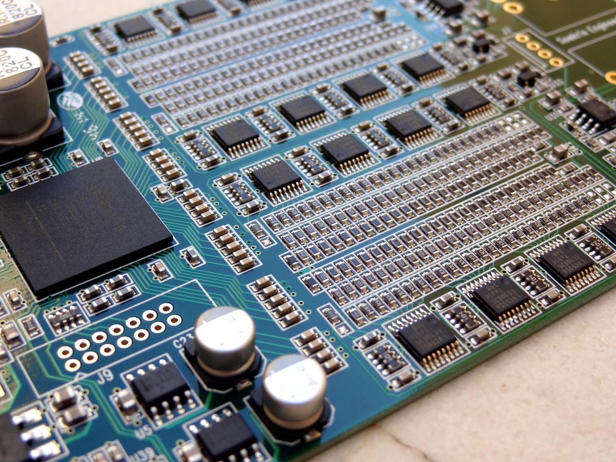
Here is a photo showing some of the details disclosed in the diyaudio thread. The LVC595A [link] are 8-bit shift registers: 7 bits on one side of the chip and the 8th bit on the other side of the chip. In this implementation the 8th bit is not used in order to optimize the layout (only using the outputs on one side of the chip) as can be seen in the photo.


The capacitor in the low pass filter (C142 in the photo) is the only capacitor in the signal path. It is a high quality C0G/NP0 ceramic. Those wishing for “higher quality” can replace/bypass with a film capacitor.
ISOLATED I2S and SPDIF INPUTS
The input is isolated with (what appears to be) TI ISO7420FE digital galvanic isolators [link]. There are 3 identical isolators resulting in 6 input lines. I think these support one I2S input and 3x SPDIF/TOSLINK/AES/EBU (I don’t know if the SPDIF lines are isolated, but there is no need for 6 isolated inputs if only the I2S is isolated). More info on isolators here [link]. Seems everyone has their favorite isolation device. Of the 4 different vendors I have surveyed, they have all been used by different audio diy implementers.
The TI ISO7420x and ISO7421x provide galvanic isolation up to 2500 V RMS for 1 minute per UL and 4242 V PK per VDE. These devices have two isolated channels. Each channel has a logic input and output buffer separated by a silicon dioxide (SiO 2 ) insulation barrier.

Built-in galvanic isolation at the input is a great idea. This gives the capability to completely isolate noise disturbance is coming from the source, including isolating ground, and since here is a FIFO reclocking stage afterwards, there is no need to worry about the small added jitter (100-200 psec RMS) that these devices would add to the data.
(update [link]) There will be two AES/Spdif inputs:
- Balanced into LVDS Receiver, can be connected directly to transformer and can be run single ended for SPDIF Coax, just a capacitor and two resistors needed when single ended 75R. To keep it isolated I recommend to always use a transformer for AES Balanced and SPDIF Single Ended inputs.
- 3.3V CMOS level input, can be connected directly to SPDIF Optical Toslink receiver.
Selection between I2S and AES/SPDIF sources can be automatic or manual with two pins that can be connected directly to a control switch. For more sources you can also just switch the inputs.
JITTER REDUCTION
A notable feature of this DAC module is the reclocking of the incoming. The design is similar in principle to Ian’s FIFO reclocker, The data is received into a configurable FIFO and then it is reclocked with a lower jitter clock.
However, Ian’s reclocker is designed for ultimate performance, whereas this reclocker is designed specifically for the DAC module and therefore matched to the requirements of the entire system (meaning, I think, the best consideration for jitter performance, cost and part count).
Here are the main differences between the two:
Ian’s FIFO reclocker
- Clock is Si570 which is the best programmable clock from Silicon Labs (.3 psec RMS jitter) [link]
- Clock drives the low jitter shift registers through a clock-fanout [link]. The jitter in the fan-out device is in the fsec range
Here is the clock board in Ian’s reclocker: the Si570 is used to clock the shift registers directly. The clock connects to a fan-out device (the chip next to the clock) and separate clock lines drive the 3 shift registers in the middle of the board.

R2R Module reclocker
- Clock is Si514 is the lower grade of programmable clocks from Silicon Labs (.8 psec RMS jitter) [link]. This is used instead of the Si570 because of power consumption (lower consumption for the Si514)
- Clock signal is transmitted through the FPGA for clock division and then to the shift registers. The added jitter in the FPGA is in the psec range. More details on the jitter through the FPGA here [link]
Here is the Si514 feeding its clock to the FPGA. The FPGA supplies the clock to the shift registers.

However, the reclocked signal in the R2R module feeds straight through the resistor ladder avoiding “several layers” of electronics as compared to a conventional implementation where the reclocked signal feeds the I2S receiver, the internal filters and other electronics of DAC chip. Internally, these “several layers” of electronics add jitter to the signal before arriving to the D/A conversion stage.
In the end, the actual jitter as seen by the resistor ladder is the cumulative jitter consisting of following components
- Clock intrinsic jitter (0.8 psec RMS)
- Jitter added by the FPGA (I think in the order of 10s psec RMS based on datasheet numbers)
- Jitter added by the shift registers in the psec order based on general data on shift registers
10s of psec RMS jitter at the resistor ladder is pretty darn good in my opinion.
Further details [link]
The details of my clocking/FIFO:
Ian’s FIFO use a fixed clock, and therefore use a large buffer to take up the difference between incoming and outgoing clock. That add a large delay, which doesn’t matter for simple audio applications but are undesirable in a number of applications, like home theater or live music.
I use a much shorter FIFO, selectable down to 1 mS, and instead adjust the outgoing clock to match the incoming clock frequency as needed, being I2S or SPDIF. The Si514 oscillator used is very low jitter and digitally programmable with a resolution of 0.026 ppb (parts per billion, not million…). It also have the feature that reprogramming inside +-1000 ppm is glitchless, ie the clock adjust very nicely to small changes.
ON-BOARD MICROPROCESSOR
The onboard microprocessor is the STM32F030 uC [link]. It is responsible for:
- Measure input clock and program the Si514 programmable clock as needed
- Initially, volume control by using a potentiometer
- More features later since this is a general purpose uC
The specific device is the 32 pin device of the family with 16 general I/O pins. I believe some of the I/O pins are available through J1
POWER SECTION
The following details have been shared about the power section of the DAC ([link], [link], [link])
- Designed to be powered by a single dual 7-8V, 5W transformer. Can also take an external +/- 7-15V DC supply. Filter capacitors are Nichicon 820uF 16V CL series
- “The LME output buffers are powered via an additional large RC filter after the main capacitors, no active regulators. With a typical PSRR of 125 db I didn’t worry much about 100/120 hz ripple, only worried about higher frequency noise on the power rails….”
- A DC-DC converter (switch mode) provides the 1.2V for the FPGA core. Every other supply is low noise linear [link]
- The most critical supply is the +/- 4V reference for the resistor ladder. This is generated by a “two step, first to +- 5V, then to +-4V by precision low noise medium current opamps”; “-4V reference is sent though an inverter with 0.01% resistors generating the +4 reference”. The references are further “filtered and buffered for each rail and channel”.
- Negative voltage is required for the output opamps and other parts of the circuit [link]
Here is a picture of the main supply section. The description is my best guess based on the information provided. I believe the digital section is powered by a DC-DC converter-regulator, except for the clock which has its own regulator.

CUSTOM FILTERS AND DIGITAL CROSSOVER
I think the ability for user-defined custom digital filters is a BIG feature for this DAC. In addition to the traditional DAC filters, one can load filters that implement crossover functions.
One of my frustrations with the ESS DAC is that I have not been able to take advantage of the custom filter facility. I am able to program everything else, except for the custom filters. Even though some claim that this feature works fine, I have not encountered any diy implementation and only one or two commercial implementations. Whether due to my own ignorance or to other factors (such as lacking documentation), fact is that there are no publicly disclosed diy successes of having implemented custom filters in the ESS DACs.
With crossover filters, there is finally a BIT PERFECT high quality DAC + digital crossover solution. More specifically, current digital crossovers if used with an external DAC of choice would add additional A/D or D/A conversions plus asynchronous sample rate conversion. Imagine a more “straight wire” implementation.

(Update [link]):
First firmware release will NOT support digital crossovers, although there will be 14 available biquads, already tested in order to support de-emphasis on SPDIF inputs. As somebody already noted, there is issue of syncronization…. I have a couple of ideas how to connect multiple boards together, but I don’t have time to implement and test before shipping the first batch. But as I already said, all firmware on the board is upgradable though a std PC serial port, I will implement it soon as my big speakers are already designed for electronic crossover use….
ES9018K2M Code Fully Tested
A new version of the code has been posted in the CODE tab [link].
This version has been fully tested with an Amanero USB interface [link] connected to the DIYINHK DAC board with an 80 MHz clock. Both PCM and DSD files of various sample rates were used together with foobar [link]

FEATURES


READ THE CODE CUSTOMIZATION SECTION
Make the proper adjustment for your specific implementation in the code.
/******************* Code Customization Section *********************/

/* First: Choose the clock frequency you have and comment the other */

#define USE80MHZ
//#define USE100MHZ

/* Second: Choose stereo or mono

   | CONFIGURATION       | #define DUALMONO | #define STEREO   |
   |---------------------|------------------|------------------|
   | Dual mono           | un-comment       | comment          |
   | Stereo              | comment          | un-comment       |
   |---------------------|------------------|------------------|    */

#define STEREO
//#define DUALMONO

/* Third, optionally choose the number of inputs. 6 is the max without
   modifying the code. You could lower the number of input choices
   here. for example if you only want to see 2 choices, modify the
   code like this: #define ICHO 2                                   */

#define ICHO 6

/* Fourth, optionally change the name of the inputs. Keep 6 characters
   Use blanks if necessary. If you use less number of inputs, only the
   top ones matter.
   */

char no0[] = "INPT-A";
char no1[] = "INPT-B";
char no2[] = "INPT-C";
char no3[] = "INPT-D";
char no4[] = "INPT-E";
char no5[] = "INPT-F";

/* These inputs choices can be virtual or real. In the ES9018 there
   were 8 data lines. One could simultanously connect one I2S/DSD input
   plus 3 additional SPDIF input (thus 4 physical inputs).
   In the ES9018K2M there are two additional input lines for SPDIF so
   one can potentially connect one I2S/DSD input plus 2 additional SPDIF
   inputs.In addition one could choose different parameters -such as the
   DPLL bandwidh or filter selection-
                                                                    */

/* Fifth, adjust the interrupt routine to match your rotary encoder by
   adjusting the mode parameter in the following routine
   (search for it in the code):

   "attachInterrupt(0, rotEncoder, LOW);"

   The mode parameter defines when the interrupt should be triggered:
       LOW to trigger the interrupt whenever the pin is low,
       CHANGE to trigger the interrupt whenever the pin changes value
       RISING to trigger when the pin goes from low to high,
       FALLING for when the pin goes from high to low.

   You can also read the following link:
   https://hifiduino.wordpress.com/2011/09/12/problems-with-rotary-encoders/
                                                                    */

/***************** End Code Customization Section *******************/
This code should also work with syllable’s DIY DAC [link] which is also described in this builders thread [link]
USB-I2S Audio-Interfaces
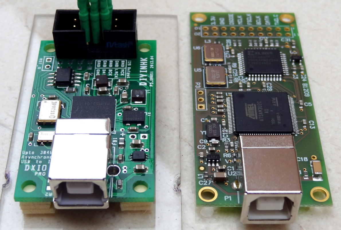
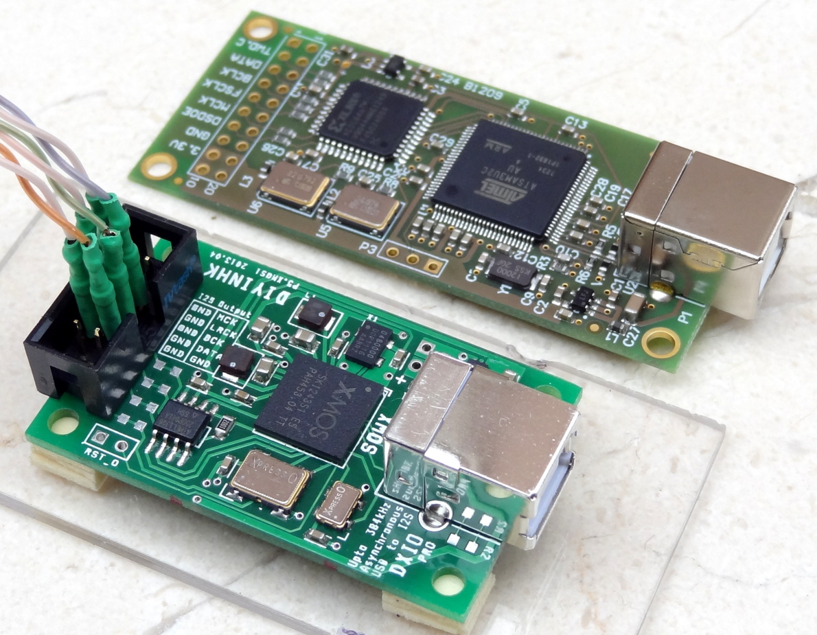
It is a great time to be an audio diy’er. There is currently great availability of quality boards aiming at providing the greatest fidelity with incredible VALUE.
Here are some side by side photos of the two USB-I2S interfaces I own.

Worthy of mention is the upcoming next generation Wave IO board. Mr. Lorien posted a sneak peek at his next generation board [link]

From the look of the layout, this board has electrical isolation of the outputs and flip-flop reclocking after the isolator.

Latest Comments