The Soekris R-2R DAC: Technical Details


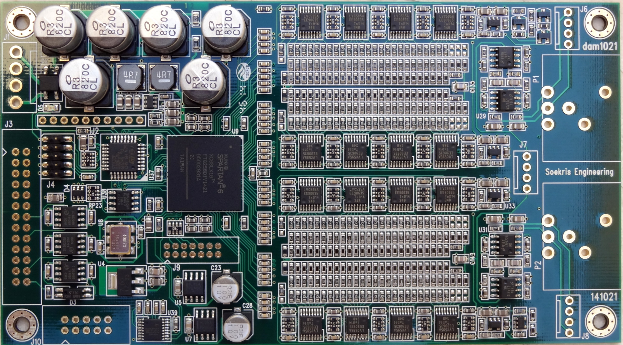
The Soekris R2R DAC is finally out, officially named
The Soekris dam1021 Sign Magnitude R-2R DAC
I will be collecting useful information here and in other posts because as the thread at diyaudio gets longer, it would be difficult to find things…
USERS GUIDE: [link]
INITIAL FEATURES
The initial release (“v1) of the firmware together enables the following features:
- I2S input up to 384KHz sample rate (tested to 192KHz)
- SPDIF input up to 192KHz (tested to 96KHz)
- Automatic De-emphasis for 44.1KHz material
- Built-in set of simple FIR filters for all sample rates
- Digital volume control through simple potentiometer
- Automatic input selection
- Data reclocking: s/w PLL with 0.02 Hz low pass filter
- S/W interface (serial interface) allows:
- Volume control (e.g. with Arduino and RS232 interface)
- Input selection (e.g. with Arduino and RS232 interface)
- Loadable FIR filters including bypass filter for NOS support (s/w utility included)
- Firmware update/upgrade
Upcoming features (through user-performed firmware upgrade)
- DSD support
- Filter cascading for digital crossover
- Filter cascading for balanced use
- Master clock output
- 4 FIR1 filters for each sample rate selectable through the serial port with a default selection (#2)
- Linear Phase
- Medium, optimized mix between Linear Phase and Minimum Phase
- Soft, mostly Minimum Phase but not that good alias rejection
- No filter, also called non oversampling, no alias rejection
- Improved response for FIR2 filter which will be modified to be pretty soft….
- Enabled TTL-level serial port on the isolated side (3.3v)
Rather than incremental updates, Soren is planning a big update [link]
USERS GUIDE: [link]
AUDIO OUTPUT
Ref: [link]
The dam1021 DAC “raw” audio output is DC-coupled. The signal out of the resistor ladder passes through a low pass RC filter consisting of a 1200 pf ceramic NP0 type (“audio” grade), and the -3db point is at ~250 Khz (different values have been reported but at this cutoff, it doesn’t really matter to the audio frequencies).
The specs of the raw output are:
- 0V offset (no need for DC blocking capacitor)
- Output level: 1.4V RMS
- Output impedance: 625 ohms, purely resistive.
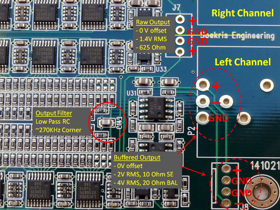
The raw output is available for single-ended connection. It is also routed to a single-ended to balanced output buffer according to the following schematic:

- LME49710: High Performance, High Fidelity Audio Operational Amplifier. Data sheet: [link]
- LME49724HighPerformance, High Fidelity, Fully-Differential Audio Operational Amplifier. Data sheet: [link]
The buffered output can be used single-ended or balanced. It can drive high impedance headphones directly.
The specifications for the buffered output are:
- Output level: 2V RMS SE, 4V RMS BAL. The output of the Differential Opamp can be used either single-ended (SE) or differential (BAL)
- Output Impedance: 10 ohm SE, 20 ohm BAL
- Output DC offset: per datasheet p.14: “The VOCM pin should be connected to ground when the desired output common-mode voltage is ground reference”. Thus based on the schematic, the DC offset = 0
Update:
Staring with Rev4 of the board, the buffered output implementation has been replaced with OPA1602 dual OpAmps: [link], due to end of life of the products that originated with National Semiconductors [link][link]. Likely the last of the engineers from the “analog golden era” have retired…
POWER SECTION
Reference: [link], [link], [link]
Main Power Section

- Designed to be powered by a single dual 7-8V AC, 5W transformer (since it has has a bridge rectifier installed)
- Can also take an external +/- 7-15V DC supply. (See section above on power supply requirements for further details)
- Actual power consumption has been measured to be 2.4W.
- Filter capacitors are Nichicon 820uF 16V CL series [link]
- Negative voltage is required for the output opamps and other parts of the circuit [link]
- A DC-DC converter (switch mode) provides the 1.2V for the FPGA core. Every other supply is low noise linear [link]
- “The LME output buffers are powered via an additional large RC filter after the main capacitors, no active regulators. With a typical PSRR of 125 db I didn’t worry much about 100/120 hz ripple, only worried about higher frequency noise on the power rails….”
Input Voltage [901]
- DC: +/- 7 to +/-15V DC; preferable 9-12V DC
- AC: 2x 7-8V AC
- Power goes though a diode bridge so polarity doesn’t matter. Connector is MTA156 type.
Maximum and Minimum Input Voltage [848]
- Upper limit of 16.5V, based on capacitor voltage and also to limit loss in linear regulators.
- Lower limit of 7.5V, based on loss though diode bridge and 5V linear regulators.
- Taking into account line voltage tolerance and transformer no/low load voltage, this results in the 7-8V AC requirement for transformers.
Power Consumption [1130]
- Positive Rail: .18A, 10V
- Negative Rail: 0.06A, 10V
- Total: 2.4W
- The positive supply draw about 3 times as much current as the negative; the current is almost independent of input voltage.
1.2V Supply
The DC-DC regulators is the TI TPS562209 [link]
Here is the reference circuit taken from the datasheet:

3.3V Supply
A 3.3V LDO Powers the Clock [link]

It is a pretty hefty regulator. And it seems the only 3.3v regulator on the board. It must also supply 3.3V to:
- 3.3V need of the FPGA
- Clean side of signal isolators
- SPDIF LVDS receivers
- Microprocessor
- Flash memory
- Other components (like the shift registers?)
Good thing it is implemented next to the clock of all places.
Reference Voltage Supply
The most critical supply is the +/- 4V reference for the resistor ladder. This is generated by a “two step, first to +- 5V (by linear regulators), then to +-4V by precision low noise medium current opamps”; “-4V reference is sent though an inverter with 0.01% resistors generating the +4 reference”. The references are further “filtered and buffered for each rail and channel”.
Linear Regulator for +/- 5V
The 8L05A and 9L05A are +5 and -5 Linear regulators [link]. Input to these regulators are the +/- rails (which could be 7 to 15V regulated or unregulated) . The outputs are filterd by 100uF capacitors.


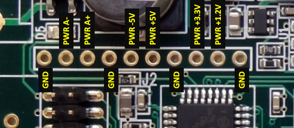
Power Rails Connector/Header [1144]
J2 is a connector to all the power rails, for testing or for supplying (limited) power to other things. The 1.2V can be used to bias the LVDS for Coax SPDIF input (see users guide)
DIGITAL FILTERS [1285]
Original (current) digital filters:
- FIR1, upsampling from incoming sample rate to 352/384 KHz in one step, with different filter length based on incoming sample rate. All FIR1 filters are basic Parks-McClellan “brick-wall” types, designed with http://t-filter.appspot.com/fir/index.html, but still shorter than your regular DAC.
- FIR1 is automatically bypassed if feeding 352/384 KHz data.
- IIR, bank of 15 bi-quads operating at 352/384 KHz, with one used for the CD de-emphasis filter, none otherwise used for the basic DAC.
- FIR2, upsampling from 352/384 KHzto 2.8/3.1 MHz, reasonable short and soft but still using same design as FIR1.
- All filters are using 32 bit coefficients, with up to 67 bit MAC accumulator.
I’m not a believer in no filters (non oversampling), but also don’t like the sharp “brick-wall” filter types with the pre-ringing. The goal is to work towards filter types that remove just enough to not cause problems with aliasing. It’s pretty easy with higher sampling rates, but is long and hard work and listening tests with 44.1 KHz, which still are the sample rate mostly used….
Further details on the filters [link]
FIR1
FIR1 is operating at 352.8K/384K (output frequency of the filter and this is set in hardware [link]) and each filter can have up to:
- 1016 tabs at 44.1K/48K input sample rate
- 508 tabs at 88.2K/96K input sample rate
- 252 tabs at 176.4K/192K input sample rate
- 124 tabs at 352.8K/384K input sample rate, but normally bypassed
This also means that:
- 44.1K/48K input sample rate, the oversampling filter must be 8X
- 88.2K/96K input sample rate, the oversampling filter must be 4X
- 176.4K/192K input sample rate, the oversampling filter must be 2X
- 352.8K/384K input sample rate, , the oversampling filter must be 1X, but normally bypassed
All upsampling is done by zero insertion, therefore gain needs to be set to match oversampling rate.
- For 44.1KHz/48KHz sample rate the upsampling is 8X, thus the gain should be 8
- For 88.2KHz/96KHz sample rate the upsampling is 4X, thus the gain should be 4
- For 176.4KHz/192KHz sample rate the upsampling is 2X, thus the gain should be 2
- For 352.8KHz/384KHz sample rate the upsampling is 1X, thus the gain should be 1 (But this filter is normally bypassed
Headroom for clipping prevention due to oversampling and the required applied gain [link]
The dam1021 have 2-4 bit of headroom though the digital filters, all the way until the volume control. So any clipping would be because of incorrect filters.
Why not one step oversampling to 2.8/3.1 MHz? [1557]
Not that practical, would require > 3000 taps. In addition, the intermediate frequency is good to have for the CD de-emphasis and crossover filters.
352K/384K is as a good compromise for the intermediate rate, so there is space for enough IIR filters for crossover use and room correction. If you go up you get less IIR filters. # filters = 45M/49M divided with intermediate rate divided with 8 = 16.
FIR2
FIR2 is operating at 2.822M/3.072M and can have up to 120 tabs, with input sample rates 352.8K/383K. The FIR2 filter don’t require much, I’m looking into doing a bessel or butterworth type filter there.
dam1021 FPGA fixed point format [link]
The filter file 1021filt.txt [http://www.soekris.dk/1021filt.skr]
There can be multiple of each filters in the 1021filt.txt filter file (part of the filter tools), but at least one (filter) needs to be there for each input sample rate. Currently just the first one for a given sample rate is used, in later firmware releases you will be able to choose between different filters
Filter tools
Filter tools and documentation will be shortly available for users to upload custom filters to the FPGA. The tools are already available here: [link]
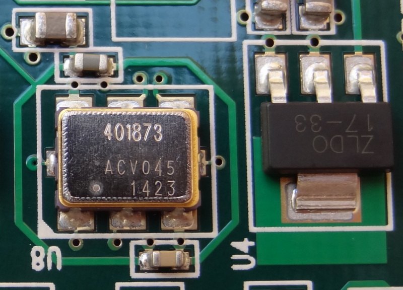
CLOCK SECTION
The clock in the dam1021 DAC is the Si514. This the lower grade of programmable clocks from Silicon Labs (.8 psec RMS jitter) [link], and according to Soren, it is well matched to the system as a whole. It is also used instead of the Si570 because of lower power consumption.

Master Clock Output Pin [848]
- I2S MCLK OUT pin: Master clock output: 45.1584 and 49.152 Mhz (which can also be divided)
- I2S FSEL IN pin: Selects between 45.1584 MHz and 49.152 MHz
Same master clock output is also used when connecting multiple DAC’s, for example for digital crossover applications.
Here is a comparison jitter measurement between the Soekris DAC and other DACs [link], [link], [link]

Jitter reduction is accomplished with signal reclocking through a short FIFO. The data is received into a configurable FIFO and then it is reclocked with a lower jitter clock, eliminating most of the incoming jitter.
Further details [link]
The details of my clocking/FIFO:
Ian’s FIFO use a fixed clock, and therefore use a large buffer to take up the difference between incoming and outgoing clock. That add a large delay, which doesn’t matter for simple audio applications but are undesirable in a number of applications, like home theater or live music.
I use a much shorter FIFO, selectable down to 1 mS, and instead adjust the outgoing clock to match the incoming clock frequency as needed, being I2S or SPDIF. The Si514 oscillator used is very low jitter and digitally programmable with a resolution of 0.026 ppb (parts per billion, not million…). It also have the feature that reprogramming inside +-1000 ppm is glitchless, ie the clock adjust very nicely to small changes.
SERIAL INTERFACE
The DAC has two serial interface:
- Standard RS232 serial interface
- TTL level Isolated Serial interface (requires firmware > 0.9)
The RS232 interface is provided by the Intersil 3221ECVZ chip [link]
The Intersil ICL3221E devices are 3.0V to 5.5V powered RS-232 transmitters/receivers which meet ElA/TIA-232 and V.28/V.24 specifications. Additionally, they provide ±15kV ESD protection on transmitter outputs and receiver inputs (RS-232 pins).
Valid RS232 levels are >+2.7V and <-2.7V according to the datasheet. Strictly speaking is > +2.4V and < -2.4V but under +/- 2.7 V it may trigger the auto power-down.
Notice that pins 9 and 11 are the TTL level serial lines to/from the FPGA. The chip convert those signals to RS232 compatible levels and provide the robustness of the RS232 standard.


Automatic power down
The chip has an automatic power-down function for noise reduction. When no valid RS-232 voltages are sensed on the receiver input for 30µs, the charge pump and transmitters power-down, thereby reducing supply current to 1µA.
The ICL32xxE powers back up whenever it detects a valid RS-232 voltage level on the receiver input. This automatic power-down feature provides additional system power savings without changes to the existing operating system.
The chip is a drop in Replacements for MAX3221E, MAX3222E, MAX3223E, MAX3232E, MAX3241E, MAX3243E, SP3243E, meaning it should be fully compatible with USB interfaces implemented with those chips.
MY OTHER POSTS ON THIS DAC
| TITLE | SUBJECT |
LINK |
DESCRIPTION |
| Soekris dam 1021 R-2R DAC ILLUSTRATED GUIDE | Users Manual | [link] | Users manual for the Soekris DAC. |
| Soekris dam1021 Build | Build Guide | [link] | Details of my initial build of the Soekris DAC. |
| dam1021 R-2R DAC MODs | Mods | [link] | Mods I have performed on the DAC build. |
| dam1021 R2R More Mods | Mods | [link] | Later mods on the DAC build. |
| Digital Filters for Soekris R2R DAC | Digital Filters | [link] | Extensive list of DIY filters from the diyaudio filter brewing forum thread. |
| R2R Benchmark Filters (for now) | Digital Filters | [link] | Latest set of filters developed and shared in the diyaudio filter brewing forum thread. The best filters of the bunch. |
| R-2R DAC For The REST of US | Technical Details | [link] | Introductory post describing the innovations and capabilities implemented in this DAC. |
| The Soekris R-2R DAC: Technical Details | Technical Details | [link] | Additional technical details of the Soekris DAC that were not covered in the post above and collected after I had the DAC on my hands. |

You should earn a medal for that summary 🙂
On post #1147 by Soekris says that left/right label are inverted on schematic – so I guess P1 is right and P2 is left.
I’m waiting the filter cascading for balanced use, to build a fully discrete balanced dac/headamp.
I guess you’ve seen dimdim forking your code to build a controller ( #994 ) ? Did you contact him or plan something like this ?
Thanks. Yes, I’ve seen dimdim’s plans. Everyone is welcomed to reuse the code :-). For now, the DAC has everything already. When more features are added, I may write some code, but no plans right now…
Thank you thank you thank you! Just saved me a few hours trawling through the topics on DIYAudio.
“Connect the dam1021 serial port to a PC serial port ”
How exactly do we do that? what kind of cable do we need?
You’ll need some inexpensive USB to Serial adapter.
provide you soldered some pin header on J10:
This inexpensive cable should do the trick with appropriate drivers installed:
http://www.ebay.com/itm/USB-To-RS232-TTL-UART-PL2303HX-Auto-Converter-USB-to-COM-Cable-Adapter-Module-/310676792112?pt=LH_DefaultDomain_0&hash=item4855c7a330
Wow, that is cheap. I got to get me one…
Should probably look for one with 3.3V signals? Some are 5V…
Nevermind… Soren confirmed it works on 5V signals for the serial port.
We may need one of these TTL – RS232 convertors?
http://www.aliexpress.com/item/Hot-Sale-MAX3232-Serial-Port-Mini-RS232-To-TTL-Converter-Adaptor-Module-Board-Free-Shipping/1779614076.html
Some of the chips seem to do RS-232 straight. Check this link: http://maxembedded.com/2013/09/serial-communication-rs232-basics/
Did you pursue getting this cable? Did it work? Looking for a smaller/neater way than the Keyspan USA-19HS I use.
No I have not. Soren indicated that he will enable the isolated serial interface in the next revision of the firmware. So far I am very happy with the standard filters and having iTunes upsample to 192KHz.
wow, really thanks. I thought I need to find a RS232 port.
I think I have the same device (described in the link) somewhere. I’ll try it and see if it works. A real RS232 port would be guaranteed to work. The DAC board has a separate chip just to handle the RS232 protocol.
Any people success to connect the dam with Macbook air? I do not have PC at home so…
@BigGear
Can you confirm successful use of the Adafruit device described in the link with the Soekris DAM1021? I noticed that some people were having trouble with other random adapters.
Thanks for the reply!
Would a pickit 2 do the trick?
While pickit2 allow UART/serial protocol, it doesn’t create a virtual COM port on your pc, so that you must find a way to do the same think that soekris describe only with pickit 2 software… because you won’t be able to use hyperterminal or any other UART software…
DAM = Digital Analog Module (maybe?)
or “Digital Audio Module”?
/U.
The wiring diagram has a small mistake – RCA SPDIF GND is drawn to PWRLED, but should go rather to GND, no?
Otherwise a terrific job!
Yes. Thank you. Corrected
Thanks! Saved me hours.
I’m quite looking forward to this: “Filter cascading for digital crossover”
I am looking forward to the filters for digital crossover too
Worth noting that the Si514 XO has an onboard LDO which is intended to make it relatively immune to PSU noise. The specs mention a jitter increase of 3.5ps with a 100mV sine wave applied to the power pin.
Thanks ! Great summary !
Looking forward to read [hopefully 😉 ] about your listening impressions, esp. in comparison to ES9018/Buffalo DAC.
please try to measure distortion with DC offset such as 50%,25% of FS.
Thanks a ton! May be this is a funny question here but could you explain more about output? I am very confusing because there are three way to get the signal out? And what is the different between raw and buffer output?
Thanks again!
Thanh
I added a diagram to the post. You can use the raw output into high impedance equipment such as preamps and amps. The buffered output can power headphones directly, but it is there mainly to provide a balanced output.
Perfect visualisation, thanks a lot Big Gear!
Excellent reference – thank you. Have you powered your board from the J2 A+ and A- pins? Any difference in sound?
I just finished the PS (12V regulated). Not hooked up yet. I don’t expect it would sound different bypassing the diode…
I’m curious too as to what 12V regulated supply you are using…care to share?
It is a HiFiduino supply. I built it 🙂
thanks…
I can’t seem to find a link anywhere on the site to it…..
It is in a new post I put out today
still can’t find it…do you have a link?
thanks…
What 12V ps are you using?
Awesome blog!! I have started a new thread over on Headfi and have shared some of your information – I hope that is OK?
Will order a board soon to begin a DAC build project.
Thanks again!
http://www.head-fi.org/t/754529/the-new-soekris-r-2r-dac-technical-details#post_11308407
Of course. Share all you want 🙂
thanks for the write ups they save lots of time
has anyone spotted the +/-4v regulation system?
Hi BigGear,
What if I have only 10VDC at J2, is it too low for dam1021?
Thanks.
Sufficient. I think the low limit is about 7V
Did you listen to it?
Regards!
I wonder if the jitter measures on the Amanero/BIII had an isolator, the other two contenders have isolated inputs and by experience I know a free DIYINHK isolator board instered between the Combo384 and the BII/III can make a huge difference in many ways. I didn’t measure jitter but I measured a +6dB increase in SNR with it inserted in the path and I guess that USB noise can get into other areas.
An isolator typically adds jitter (~100s psec), but reduces unwanted noise.
Wouldn’t it add jitter only if one is using the Amanero’s XOs? If the onboard BIII is being used there should be no increase in jitter, right?
In theory, the BIII on board clock would “eliminate” the added jitter. I think jitter measurement is very hard. There are many factors involved including your test set-up, etc.
Great writeup. One minor nit. In the Reference Voltage Supply section, it says “-4V reference is sent though an inverter with 0.01% resistors generating the +4 reference”. I do not think this is correct. There are actually 4 opamps. Two generate +4V, and two generate -4V. These four voltages feed the 4 rows of shift registers. -4V connects to the SR gnd pin, and ground connects to the SR VCC pin, if you’re wondering how you power a SR with -4V.
Randy
Awesome info, thanks. Regarding the filters, how exactly do you disable the filters (i.e. switch on NOS mode), for use with 96 kHz material? Maybe there is a link with instructions somewhere…
Thanks!
Some of the filter collections contain a NOS filter…
Fixstone Computer Service
Payday loans
toms Norge
Home Solar Power
kitchen remodeling northern virginia
If you are a purchaser of the rev 1, see this thread on DiyAudio:
http://www.diyaudio.com/forums/digital-line-level/294351-soekris-sonics-comparisons-other-stuff-5.html#post5110663
Original purchasers of the rev 1 dac boards purchased them assuming, based on the initial sales pitch, that they were finished, tested, functions as advertised, products. Only afterwards did Soekris Engineering admit they were beta tests boards with design issues and did not live up to his initial claims. He has refused to offer any refunds, credits, etc. despite a classic bait and switch.
If you were a victim of Soekris Engineering’s dishonest business practices, contact me.
Can I simply say what a reduction to search out someone who actually is aware of what theyre speaking about on the internet. You definitely know the right way to deliver a problem to light and make it important. More people must learn this and perceive this facet of the story. I cant believe youre not more common since you positively have the gift.