Archive
First One Build: Power Supply Selection
LC tested three First One amplifiers, each one equipped with different power supply [link]:
AB comparison 1: Single Connex vs Dual AudioPower
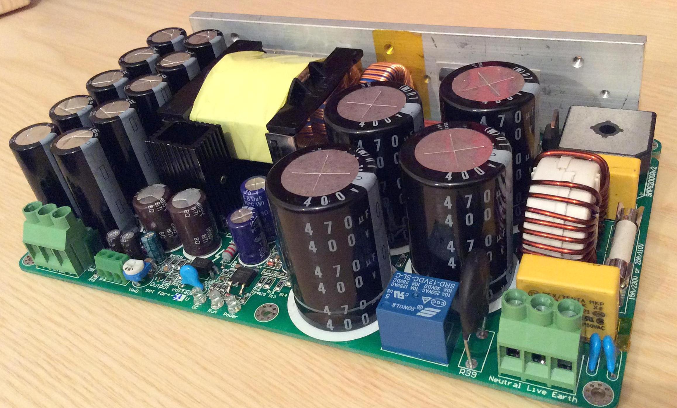

It was not really hard to recognize the better PS, since bass was really on a weak side of Connex, probably the reason lies in the use of a single SMPS2000R for both amp’s channels, nevertheless the sound-stage was narrow, instruments weakly presented, thin bodies, no real feeling of involvement into the music. DPS-500/63 were in dual mono configuration, meaning one per channel. Transparency and details resolution was very similar but the bass was one step ahead over the Connex. Still no real musical involvement presentation here, sound more or less stuck to the speakers, instruments with weak bodies, sound-stage not well formed.
Since both were regulated SMPSs we got an impression that the problem lies in the voltage regulation principle, too much interfering in audio signal is probably the worst thing it could happen from amp’s power supply.
It is interesting to point out that without AB comparison, LC had this to say about the Connex supply:
Cristi, your second SMPS2000R is just WOOOW, driving both channels. This is the one packed with Rubycons on primary and secondary side, set to +/-63 V, no hum, dead quiet silence, rock stable imaging, resolution is at the top notch, no sign of sibilants on vocals, liquid like sound, bass is simply awesome, like a day and night different from first one tried, also much better than SMPS1200 [link]
Yes, a day and night between the two SMPS2000R, named them A and B versions. As I can see the only difference is in secondary cap bank, maybe also something else, surely Cristi would have something more to say about them. Anyway version B with Rubycons is an absolute winner up to now, doubtless.
SMPS1200 provided better bass than Cristi’s A version, but that’s about it, both Connex gives higher headroom, also more power because of higher and regulated rail’s potential, at the end resulting in more stable sound imaging. [link]
AB comparison 2: Single Hypex vs Dual AudioPower

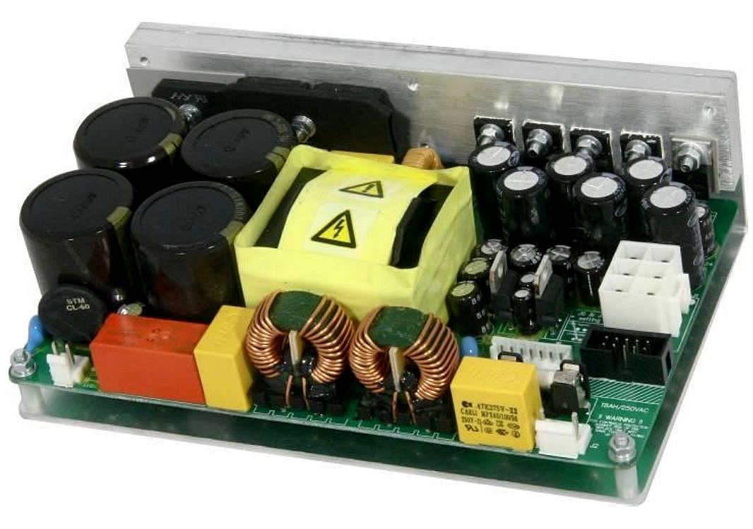
Here is the latest version of the Hypex supply. The entire PCB was updated in 2013 according to the data sheet [link]
After half an hour of mental pause, test continued between (single) Hypex SMPS1200A400 and (dual) Audio Power DSP-500/63. First we listened to DPS-500/63, musical impression stayed very much the same as it was in the first session. Weak presentation left us more or less cold, music is simply too thin, uninvolving.
Hypex’s turn then settled the things where they should belong, suddenly real music in the room. It was immediately clear to all of us who’s having magic stick in its sleeve. SMPS1200A400 shocked us with music so real that the other two seemed like that there was something broken in them.
Hypex presented bass so low and strong that our jaws just dropped for a while, dense wall of air moved with lowest possible frequencies we could still hear, still with ease. Sound-stage completely another story from previous contenders, no speakers in the room only musicians and instruments, this time with fully developed bodies, atmosphere of a recording stage, whether real or artificial, presented in full scale. SMPS1200A400 puts the First One amplifier in the first league of power amplifiers no matter the price level.
AB comparison 3: Single vs Dual SMPS1200A400 [link]

The result is not so far from our expectations, tight similarity with very slight differences noticeable on momentary A-B test; otherwise, on not so closely conducted comparisons, it would be very hard or even impossible to distinguish the two configurations.
In which cases to choose single or double SMPS solution greatly depends on the speaker’s efficiency and impedance, these two parameters dictate how power hungry your speakers are and of course how loud you want them to be.
The ultimate and preferred First One solution is still dual mono configuration, although the use of a single SMPS completely fulfills the needs in a smaller system.
AB comparison 4: Linear vs AudioPower [link] (Comparison on-going…)

Conclusion
Well, after the not-so-subtle remarks in the AB comparison performed by LC, it is almost impossible to argue the fact that using anything else than a Hypex SMPS1200A400 supply would “rob” performance out of the amplifier modules. A plus is that the amp modules are factory calibrated and tested with this supply in mind. In addition, especially for a budget-constrained build, the AB comparisons also showed that unless there is a need for high current demand, a single SMPS1200A400 would sufficiently fulfill the designed performance of the First One amp. Further, the Hypex SMPS1200A400 is competitively priced against the other two offerings.
Best choice
If one wishes to confirm the results or adjust certain variables in the comparisons, it would be difficult for the diyer to replicate even some of the tests reported by LC. First several amps were configured with the different supplies for a immediate AB comparison. Second, one would have to procure the different supplies for the test. This would be cost prohibitive for the common diyer. In addition Hypex has a long and excellent reputation for high end audio not just a a provider of high fidelity products but also as a technical innovator, and thus there is very little chance to find a superior supply for this application.
Why Hypex supply outperforms Connex supply?
Having examined the Connex supplies in detail, I find that the use of soft switching approach minimizes the generation of EMI while increasing efficiency. The hypex datasheet does not say whether it is a “soft” or “hard” switching approach. It merely says “The SMPS1200 is optimized from the first phase of design to final implementation to realize the lowest possible EMI signature required of the most demanding audio applications” this could very well mean the use of soft-switching and/or more aggressive output filtering. So from a SMPS switching approach point of view, one cannot say why one would sound better than the other.
Therefore, the difference in audio quality seems to be fully attributed to the unregulated output nature of the Hypex supply. This comes as a surprise because the audio implementations have been moving toward regulation and now we find that SMPS with regulated output seems detrimental to audio quality at least in this instance.
LC believes that regulation “interferes” with the audio signal [link]
For those interested in more technical details, the Connex supplies were tested extensively [link]. And even thought they exhibit superb performance and I remain a fan of Connex supplies [link], I cannot justify using them with the First One Amp modules in light of the comparison presented here.
AudioPower develops Unregulated PS
It is worthwhile to note that AudioPower has recently developed Unregulated versions of their Audio SMPS, perhaps a testament that “unregulation” has sonic advantages (or just competing with Hypex). [link]. I’ll have to admit, they are best looking.

My initial choice
For now I will use the power supply of the Adcom GFA-5300 AM. It generates +/- 52 volts and according to spec, can supply a max of 720VA

First One Build: Heatsink Selection
One of the most important parameters for proper operation of the Fist One amplifier module is adequate heat dissipation through a large enough heatsink. The amp module operates in class AB with an idle current of 280 mA.
The idle dissipation of the First One is >30 W at +/-63 V, plus audio power dissipation easily adding extra 50-70 W, so 100 W all together to dissipate.
To calculate the temperature of the heatsink during operation: 100 W * 0.5 K/W=50 K added to room temperature (25 C) resulting in 75 C heatsink temperature. At that point silicon die in output transistor is around 100 C and that is somehow at max acceptability. To calculate idle temperature: 30W* 0,5 K/W=15 K (or C) added to room temperature resulting in 40 C. [link]
Supply DC current to the First One module without input signal present (idle current) is 280 mA, multiplying it with 120 V rails potential, gives 33.6 W of total quiescent power dissipation per module, so in stereo total 67,2 W. That is serious thermal loading for the chassis and heatsink if one would want amp to be below 45 degrees in a room environment. [link]
LC recommends “any heatsink having 0,5 K/W or even lower”. Something like Fischer Elektronik FK157 [link]. Below are the heatsink profiles of the FK157 and other similar profiles that will yield 0.5 K/W dissipation or better. These were extracted from the Fischer Elektronik catalog [link]

Notice that by comparing the 3 profiles shown above, in order to achieve a 0.5 K/W dissipation you would need:
- 2″ of SK501
- 2″ of SK 586
- 2″ of SK 157
Seems longer fins only help if you need a dissipation factor lower than 0.5 K/W or even lower than 0.3K/W
Even a shorter profile would yield a dissipation rate of 0.5 K/W. In this example a 4″ heatsink would achieve a dissipation rate of 0.5K/W

The Semelab application note has a extensive section on heatsink selection [link]. If you read the whole thing, basically the bottom-line thing to do is that the heatsink shall not exceed 70C during operation.
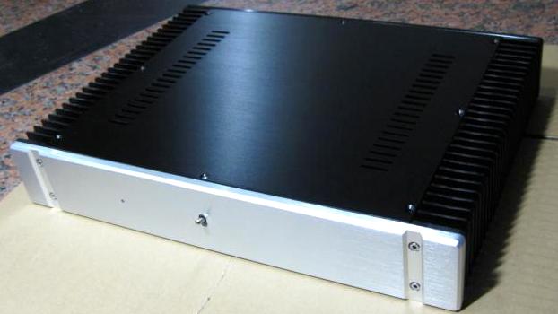
Factory Chassis
LC provides appropriate heatsinks as part of the factory chassis (which cost Euro 300 plus shipping). Following are the photos of the “factory” heatsinks ( I think they are SK 157 with height 70 mm, so having a dissipation coefficient of a bit less than 0.4K/W). The chassis is beautiful and built like a tank. If you want the best, this is it.


In order to obtain the factory heatsinks, you need to purchase the chassis (300 euros plus shipping – I would think US$60-$100 for shipping based on eBay examples. So total cost would be US$450-$500) [link]:

Although it is highly desirable to have an enclosure that is built at the same high standards as the amp module, if budget does not permit, there are other options.
Chinese chassis from eBay
The is the the lowest cost for a chassis plus heatsink meeting the required dissipation rate [link]. This case costs about US$ 160 including shipping.
The heatsink size for this case is 300x50x67mm with a profile similar to SK501 but with the fins 10 mm longer. At 67 mm height, Likely it exceeds the required 0.5 K/W dissipation rate. It probably rates at 0.45K/W. (This is just theory in practice you may need a larger (taller) heatsink depending on different factors such as ambient temp, etc)
You can find an example implementation of this case with the VSSA amp here [link].
A similar but with taller heatsinks can be found here [link] and here [link]
Heatsink Only
If you want the minimum cost and If you live in the USA, a good source is “HeatsinkUSA”. High quality and good prices. The largest one seems to fit the bill [link]. Specs are:
- Width is 10.080″
- Fin Height is 2.5″
- Base Height is .375″
- Weight is approximately .99 lbs per inch
- C/W/3″: approximately .80 (for a 3″ heatsink)

This heatsink is similar in profile to SK524 above except it has one less fin but the fins are much larger at 50 mm. If we use the dissipation curve of the SK524 we find that a 4″ heatsink will meet the required 0.5K/W dissipation. Note that the published thermal dissipation specification for this heatsink is 0.8 s for a 3″. If we go by the dissipation curves shown in the Fischer Elektronik catalog, then this values seems too conservative. But in order to be safe, a 5″ heatsink would likely be more than sufficient. A pair of 5″ heatsinks would set you back about $90 including shipping.
Thrift Store Amp
Even cheaper than getting heatsink is using an old amp from a thrift store. If you are lucky, you may find an old amp with large heatsinks. I had purchased a used Adcom GFA-5300 amplifier from the local thrift store for $15. This was a few years back. nowadays, even thrift stores are drastically increasing the price of used audio equipment. I would say this amp would probably sell for $50 if bought today.
The heatsink of the Adcom has the following dimensions:
Width: 200 mm; height: 90 mm; depth (fins): 55 mm; base plate thickness: 5 mm; number of fins: 20.


The closest profile I could find from the Fischer Elektronik catalog is the following:

As can be seen, the Adcom heatsink is a bit wider, the fins a tad longer and it has 4 more fins. I would say at 90 mm in height, it would easily meet 0.6K/W. but it does not meet the minimum requirement of 0.5K/W.
Using the power supply of the Adcom Amplifier
What if we use the power supply of the Adcom which provides +/- 52V? We can calculate the required heatsink dissipation with this supply by following the example given at the beginning of this section and the following requirement [link]:
As we don’t want to have more than 45 C in idle, please use heatsink having thermal coeficient of 0,5K/W or less for each channel.
First One module has 35 W idle power dissipation when supplied from +/-63 V PSU.
The idle current of the Amp is 280 mA (how to measure [link]). Even at a lower supply voltage this bias requirement is fixed [link]
Thus at +/- 52V supply we get 29 Watts. With a heastsink of 0.6K/W we get 29*0.6=17.4 C. Adding the room temperature of 25C we get 42.4K which is within spec but this is only at idle.
The service manual of the Adcom Amp gives this power data:
I plan to use this Adcom amp for my first build. It seems to have adequate heatsinks. I will have to build up the amp to know for sure.
Summary of choices
- Factory case: ~$450-$500
- eBay Chinese case: ~$150-$200
- Heatsink Only: ~$90
- Thrift Store Amp with large heatsinks: ~$30-$60
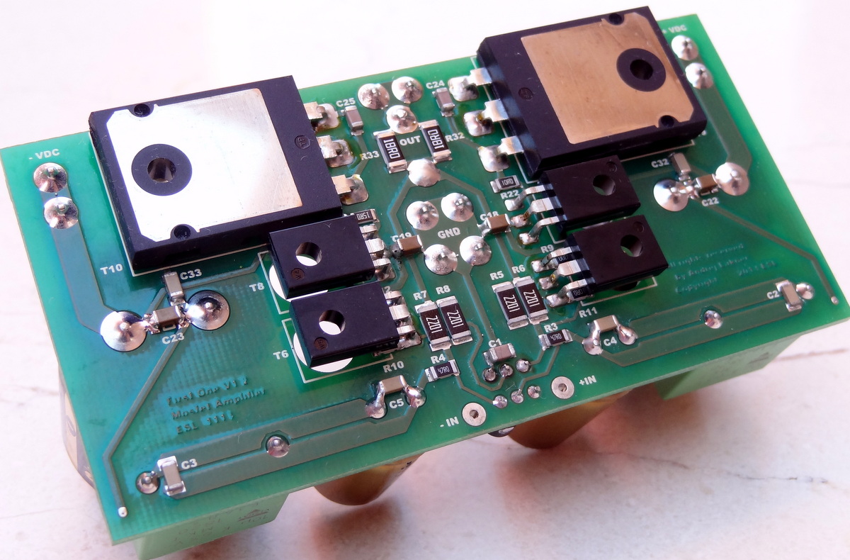
First One Amplifier Module
The First One Amp module [link] is a high performance (High Fidelity?) and yet very affordable class AB current-feedback amplifier module. It establishes a benchmark for price/performance.
Developed by “Lazy Cat” (LC) at diyaudio, it is the big-brother commercial version of the DIY VSSA (“Very Simple Symmetric Amplifier) [link] and incorporates all the knowledge obtained from that project. Whereas the VSSA was fully open and fully diy, the First One amplifier is available as a factory built and tested module. Available for diyers as well as OEM to manufacturers, the module has been seen in a finished amplifier for a road show in Slovenia [link].
Photo of First One’s little brother: completed VSSA module (built by LC):

FIRST ONE MODULE
Since I am new to this module and was not aware of the VSSA, I’ll use this and following post to gather my knowledge for my amplifier build. The information is mostly from the diyaudio threads, but there it is spread out all over the place and hard to find.
Photos of the First One Amplifier Module.

Use of name-brand “audio grade” components…

The current version is V1.2. There is a V1.3 that has been developed but not quite yet available for sale. For those of us with V1.2, LC has promised to send modding instructions but only to those that have completed the build of the amp.

Thermal coupling for these two transistors. The schematic is not public since this is a commercial product.
Notice the adjustment pots (TRx) and the measuring points (TPx)

Output Power transistors are Semelab “ALFET” double die MOSFET N and P-channel pair, rated at 250 W and 16 Amp continuous current. These are specially designed for audio applications [link]:
- The N-channel device is: ALF16N16W/ALF16N20W [link]
- The P-channel device is: ALF16P16W/ALF16P20W [link]


SPECIFICATIONS
Module Size
100 x 50 x 40 mm (W x D x H). [link]
Supply Voltage
+/-40 V to +/-63 V
DC coupled
The amp modules are DC coupled, no capacitor in front of the input stage.
Measurements
I’ll compare the specifications of the First One module (FO) [link] vs an old Hitachi amp [link] and an Adcom amp:
| Parameter | First One |
Hitachi HMA-7500 |
Adcom GFA-5300 |
| Max Power 8 Ohm | 150 Watt 0.05 THD | 80 Watt 0.005 THD | 80 Watt 0.018 THD |
| Max Power 4 Ohm | 230 Watt 0.05 THD | 80 Watt 0.005 THD | 125 Watt 0.018 THD |
| Bandwidth | 3 Hz to 3 MHz (-3dB) | 5 Hz to 100 KHz (-1dB) | 3 Hz to 130KHz (-3dB) |
| THD | 0.0034% (100 Watt) | <0.005% (80 Watt) | 0.02% (125 Watt, 1KHz) |
| IMD | 0.003% | <0.008% | <0.07% |
| SNR | 110 dB | 118 dB | >100 dB |
| Input Impedance | 10 Kohm | 47 Kohm | 50 Kohm |
| Damping Factor | >2000 (4 ohm) | 100 (8 ohm, 1KHz) | >350 |
| Year Introduction | 2014 | 1980 | 1995 |
According to published specifications, the First One amp has very impressive specifications and overall best of the bunch. The old Hitachi has still has very impressive specifications (but at a much lower max power).
Damping factor
Measurements performed in order to determine Zout and consequently the damping factor (DF). A sinusoidal signal of 100 Wrms at 20 Hz, 1 kHz and 20 kHz was passed onto a 4.08 Ohm load resistor, measured with FLUKE 289 True RMS Multimeter and here are the results. [link]
20 Hz, 100 Wrms/4.08 Ohm:
- DF(20 Hz)=Rload/Zout=4.08 Ohm/0.00121 Ohm=3372
1 kHz, 100 Wrms/4.08 Ohm:
- DF(1 kHz)=Rload/Zout=4,08 Ohm/0,0004 Ohm=10200
20 kHz, 100 Wrms/4,08 Ohm:
- DF(20 kHz)=Rload/Zout=4,08 Ohm/0,00162 Ohm=2519
Very large damping factor by itself likely means that the amp itself would not be the limiting factor for controlling the oscillations in the speaker. This means that other factors (such as speaker cable impedance) would contribute more to the damping factor seen by the speaker. The speaker’s own impedance is the mayor contributor…
A PERFECT MATCH WITH R2R DAC?
Seems a perfect match for the upcoming discrete R2R DAC. The amp being single-ended (and DC-coupled) can take the output signal straight out of the resistor ladder. In addition, being wide-band would further benefit from R2R conversion (as opposed to delta-sigma) because the R2R DAC does not generate high frequency noise.
R-2R DAC For The REST of US
A MOST INTERESTING DIY PROJECT IN A LONG TIME
A Discrete R-2R Sign Magnitude 24 bit 384 Khz DAC [link].
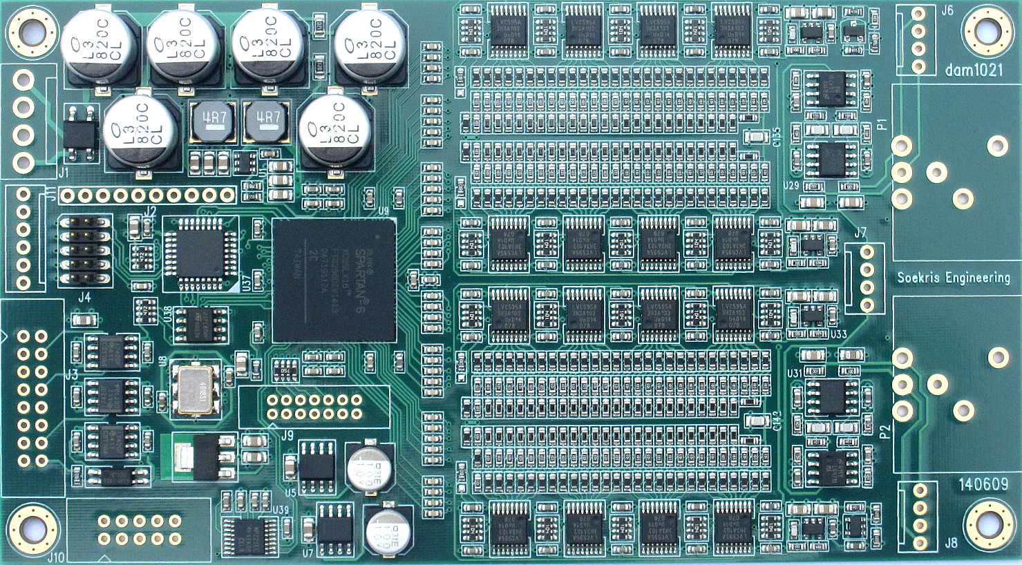
The DAC Module includes all local power supplies, a programmable low jitter clock, Micro-controller and balanced output buffer. It is implemented on a 4-layer PCB. The board size is 3.2″ x 5.8″ (81 x 147 mm).
As the industry migrated from R2R topologies to Sigma-Delta in their quest for higher bit-depth, higher performance (and cost management), present implementations of R2R DACs are pretty much hand-crafted commanding a high premium.
As the author states:
“I believe that the sound quality will be the absolute best, better than any Delta Sigma DAC, in class with discrete DAC’s from totaldac and msb technology. And for way way less cost :-)”
For the rest of us with limited resources wanting to experience a ladder DAC, this is the DAC to have.
An excerpt from the PCM1704 [link] datasheet expunds the good points of a ladder DAC:
Digital audio systems have traditionally used laser-trimmed, current-source DACs in order to achieve sufficient accuracy.
However, even the best of these suffer from potential low-level non-linearity due to errors in the major carry bipolar zero transition. Current systems have turned to oversampling data converters, such as the popular delta-sigma architectures, to correct the linearity problems. This is done, however, at the expense of signal-to-noise performance, and the noise shaping techniques utilized by these converters creates a considerable amount of out-of-band noise. If the outputs are not properly filtered, dynamic performance of the overall system will be adversely effected.
The PCM1704 employs an innovative architecture which combines the advantages of traditional DACs (e.g., excellent full-scale performance, high signal-to-noise ratio, and ease of use) with superior low-level performance.
Granted, that was circa 1999. Since then the Sigma-Delta camp has made great strides. Even so, R2R DACs have not lost their appeal as witnessed by the interest in this project and the current commercial offerings.
TARGET PRICE
The DAC module is not yet available for sale. The target price is US$240 with 0.02% resistors. This is a steal considering how much other R2R implementations cost.
ADVANCING THE STATE OF THE ART
The last commercially available R2R DAC chips were the PCM1704 [link] and the AD1865 [link]. They have been out of production for a long time but still available for purchase for example here [link] and here [link].
Here is a table comparing selected performance numbers and features as described in the data sheets and by the author in the diyaudio discussion thread.
- The PCM1704 is typically used withe a companion chip, the DF1704 [link].
- The AD1865 is also used with a companion filter chip such as the Sony CXD1244S [cxd1244s]
| Parameter | Seokris R2R |
PCM1704+DF1704 | AD1865+Digital Filter |
| Max Input Sample Size | 24bit | 24bit | 18bit |
| Max Input Sample Rate | 382KHz | 96KHz | 44KHz |
| Max Resolution | 28bit (1) | 24bit | 18bit |
| Inputs (2) | 1x Isolated I2S, 3x SPDIF/TOSLINK/AES/EBU [link]; future DSD upgrade | Serial only (DF1704: LJ, I2S) | Serial only through the digital filter chip |
| S/W Interface | Serial (Not I2C) | Serial (Not I2C) | Depends on filter chip |
| Oversampling Filter | On-board built-in and user defined (3) | Sharp, Slow roll-off (DF1704) | Needs External Filter |
| Channels | 2 – Stereo | PCM1704 is single channel, so DF1704+2XPCM1704 | 2 – Stereo |
| Jitter Reduction | Re-clocking input data through a FIFO Buffer (similar in design to Ian’s FIFO [link]). Uses a low jitter (0.8 psec RMS) Si514 programmable clock [link] which drives the LVC595 shift registers after clock division in the FPGA (Si514 -> FPGA divider -> LVC595) | None | None |
| Output | “Raw” single-ended voltage output (1.4V RMS, 1.25 Kohm) or buffered balanced voltage output using TI LME49710 + LME49724 [link] | Single-ended current output | Single-ended current output or buffered single-ended voltage output |
| Jitter Reduction | FIFO Buffer and reclock with low jitter clock | None | None |
| THD+N (0db) | 0.0063% .05% resistors (Module measurement) | 0.0008% K-Grade (PCM1704 spec) | 0.003% J/K Grade (AD1865 spec) |
| THD+N (-20db) | – | 0.006% K-Grade (PCM1704 spec) | 0.01% J/K Grade (AD1865 spec) |
| THD+N (-60db) | 0.37% .05% resistors (Module measurement) | – | 1% J/K Grade (AD1865 spec) |
| SNR | 126 dB (Link) | 120 dB | 110 dB |
Notes
(1) The Soekris R2R implements 28 bits of internal resolution in order to provide sufficient headroom to allow for a “perfect digital volume control. At -72 db volume you still have 16 bit resolution with perfect linearity” [link].
(2) The PCM1704 and AD1865 are NOS ladder DACs expecting an input stream from an external filter device such as the DF1704 [link]. Therefore they typically cannot accept and I2S input format. The input format for those chips consists of a clock signal, data signal and data latch signal. More information can be found in Ian’s “I2S to PCM” board project [link].
(3) The oversampling filter is implemented in the on-board Spartan-6 LX16 FPGA. It has 15K logic cells and can be configured as having 8 full high resolution MAC’s by using its 32 DSP48A1 MAC blocks in groups of 4 allowing them to do 35 x 35 bit multiplications plus 70 bit summers. Two of these hig-res MACs can be used for the first 2 most critical oversampling FIR filters; running them at just 49.152 Mhz makes space for 1024 coefficients if needed, then 2 more for the rest of the FIR filters. The rest for other functions, like de-emphasis, volume control and digital crossover filters… [link]. The user can use generate the filter coefficients and upload them to the FPGA [link]
Filter tools:
Here is a photo showing some of the details disclosed in the diyaudio thread. The LVC595A [link] are 8-bit shift registers: 7 bits on one side of the chip and the 8th bit on the other side of the chip. In this implementation the 8th bit is not used in order to optimize the layout (only using the outputs on one side of the chip) as can be seen in the photo.


The capacitor in the low pass filter (C142 in the photo) is the only capacitor in the signal path. It is a high quality C0G/NP0 ceramic. Those wishing for “higher quality” can replace/bypass with a film capacitor.
ISOLATED I2S and SPDIF INPUTS
The input is isolated with (what appears to be) TI ISO7420FE digital galvanic isolators [link]. There are 3 identical isolators resulting in 6 input lines. I think these support one I2S input and 3x SPDIF/TOSLINK/AES/EBU (I don’t know if the SPDIF lines are isolated, but there is no need for 6 isolated inputs if only the I2S is isolated). More info on isolators here [link]. Seems everyone has their favorite isolation device. Of the 4 different vendors I have surveyed, they have all been used by different audio diy implementers.
The TI ISO7420x and ISO7421x provide galvanic isolation up to 2500 V RMS for 1 minute per UL and 4242 V PK per VDE. These devices have two isolated channels. Each channel has a logic input and output buffer separated by a silicon dioxide (SiO 2 ) insulation barrier.

Built-in galvanic isolation at the input is a great idea. This gives the capability to completely isolate noise disturbance is coming from the source, including isolating ground, and since here is a FIFO reclocking stage afterwards, there is no need to worry about the small added jitter (100-200 psec RMS) that these devices would add to the data.
(update [link]) There will be two AES/Spdif inputs:
- Balanced into LVDS Receiver, can be connected directly to transformer and can be run single ended for SPDIF Coax, just a capacitor and two resistors needed when single ended 75R. To keep it isolated I recommend to always use a transformer for AES Balanced and SPDIF Single Ended inputs.
- 3.3V CMOS level input, can be connected directly to SPDIF Optical Toslink receiver.
Selection between I2S and AES/SPDIF sources can be automatic or manual with two pins that can be connected directly to a control switch. For more sources you can also just switch the inputs.
JITTER REDUCTION
A notable feature of this DAC module is the reclocking of the incoming. The design is similar in principle to Ian’s FIFO reclocker, The data is received into a configurable FIFO and then it is reclocked with a lower jitter clock.
However, Ian’s reclocker is designed for ultimate performance, whereas this reclocker is designed specifically for the DAC module and therefore matched to the requirements of the entire system (meaning, I think, the best consideration for jitter performance, cost and part count).
Here are the main differences between the two:
Ian’s FIFO reclocker
- Clock is Si570 which is the best programmable clock from Silicon Labs (.3 psec RMS jitter) [link]
- Clock drives the low jitter shift registers through a clock-fanout [link]. The jitter in the fan-out device is in the fsec range
Here is the clock board in Ian’s reclocker: the Si570 is used to clock the shift registers directly. The clock connects to a fan-out device (the chip next to the clock) and separate clock lines drive the 3 shift registers in the middle of the board.

R2R Module reclocker
- Clock is Si514 is the lower grade of programmable clocks from Silicon Labs (.8 psec RMS jitter) [link]. This is used instead of the Si570 because of power consumption (lower consumption for the Si514)
- Clock signal is transmitted through the FPGA for clock division and then to the shift registers. The added jitter in the FPGA is in the psec range. More details on the jitter through the FPGA here [link]
Here is the Si514 feeding its clock to the FPGA. The FPGA supplies the clock to the shift registers.

However, the reclocked signal in the R2R module feeds straight through the resistor ladder avoiding “several layers” of electronics as compared to a conventional implementation where the reclocked signal feeds the I2S receiver, the internal filters and other electronics of DAC chip. Internally, these “several layers” of electronics add jitter to the signal before arriving to the D/A conversion stage.
In the end, the actual jitter as seen by the resistor ladder is the cumulative jitter consisting of following components
- Clock intrinsic jitter (0.8 psec RMS)
- Jitter added by the FPGA (I think in the order of 10s psec RMS based on datasheet numbers)
- Jitter added by the shift registers in the psec order based on general data on shift registers
10s of psec RMS jitter at the resistor ladder is pretty darn good in my opinion.
Further details [link]
The details of my clocking/FIFO:
Ian’s FIFO use a fixed clock, and therefore use a large buffer to take up the difference between incoming and outgoing clock. That add a large delay, which doesn’t matter for simple audio applications but are undesirable in a number of applications, like home theater or live music.
I use a much shorter FIFO, selectable down to 1 mS, and instead adjust the outgoing clock to match the incoming clock frequency as needed, being I2S or SPDIF. The Si514 oscillator used is very low jitter and digitally programmable with a resolution of 0.026 ppb (parts per billion, not million…). It also have the feature that reprogramming inside +-1000 ppm is glitchless, ie the clock adjust very nicely to small changes.
ON-BOARD MICROPROCESSOR
The onboard microprocessor is the STM32F030 uC [link]. It is responsible for:
- Measure input clock and program the Si514 programmable clock as needed
- Initially, volume control by using a potentiometer
- More features later since this is a general purpose uC
The specific device is the 32 pin device of the family with 16 general I/O pins. I believe some of the I/O pins are available through J1
POWER SECTION
The following details have been shared about the power section of the DAC ([link], [link], [link])
- Designed to be powered by a single dual 7-8V, 5W transformer. Can also take an external +/- 7-15V DC supply. Filter capacitors are Nichicon 820uF 16V CL series
- “The LME output buffers are powered via an additional large RC filter after the main capacitors, no active regulators. With a typical PSRR of 125 db I didn’t worry much about 100/120 hz ripple, only worried about higher frequency noise on the power rails….”
- A DC-DC converter (switch mode) provides the 1.2V for the FPGA core. Every other supply is low noise linear [link]
- The most critical supply is the +/- 4V reference for the resistor ladder. This is generated by a “two step, first to +- 5V, then to +-4V by precision low noise medium current opamps”; “-4V reference is sent though an inverter with 0.01% resistors generating the +4 reference”. The references are further “filtered and buffered for each rail and channel”.
- Negative voltage is required for the output opamps and other parts of the circuit [link]
Here is a picture of the main supply section. The description is my best guess based on the information provided. I believe the digital section is powered by a DC-DC converter-regulator, except for the clock which has its own regulator.

CUSTOM FILTERS AND DIGITAL CROSSOVER
I think the ability for user-defined custom digital filters is a BIG feature for this DAC. In addition to the traditional DAC filters, one can load filters that implement crossover functions.
One of my frustrations with the ESS DAC is that I have not been able to take advantage of the custom filter facility. I am able to program everything else, except for the custom filters. Even though some claim that this feature works fine, I have not encountered any diy implementation and only one or two commercial implementations. Whether due to my own ignorance or to other factors (such as lacking documentation), fact is that there are no publicly disclosed diy successes of having implemented custom filters in the ESS DACs.
With crossover filters, there is finally a BIT PERFECT high quality DAC + digital crossover solution. More specifically, current digital crossovers if used with an external DAC of choice would add additional A/D or D/A conversions plus asynchronous sample rate conversion. Imagine a more “straight wire” implementation.

(Update [link]):
First firmware release will NOT support digital crossovers, although there will be 14 available biquads, already tested in order to support de-emphasis on SPDIF inputs. As somebody already noted, there is issue of syncronization…. I have a couple of ideas how to connect multiple boards together, but I don’t have time to implement and test before shipping the first batch. But as I already said, all firmware on the board is upgradable though a std PC serial port, I will implement it soon as my big speakers are already designed for electronic crossover use….
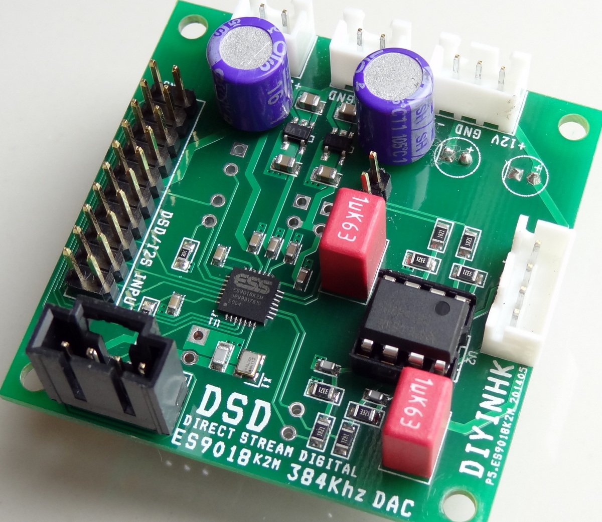
BUILDING THE DIYINHK ES9018K2M
I have come to the realization that audio diy never ends. There is never the “final” project. There is always tweaking, a new mod, new stuff. Thus I decided to use a cardboard box as an enclosure. Much easier to work with, simple tools would do.
Many would consider a proper enclosure a must for a diy project, but for me this is good enough. Here is a nice looking Lenovo tablet box.

POWER SUPPLY TRANSFORMERS
Three separate transformers were used:
- DAC supply transformer: salvaged from an VCR from the time that linear supplies were still being used. These transformers are very nice, having at least 2 hefty 9V secondaries. The secondaries feed a TPA dual PS which is used as a pre-regulators for the DAC supplies. The two capacitors hanging off the transformer provides DC to an LED (to indicate power 0n/off)
- Analog supply transformer: 15×2 toroidal transformer. (Got it from Twisted Pear Audio)
- Controller transformer: 6V DC salvaged from a wall-type supply, upgraded the smoothing capacitors


Water bottle caps are perfect for the feet.

DAC AND ANALOG SUPPLIES
Used a quad-supply board. This board is designed to provide 4 x 3.3V/5V regulated output. Two supplies receives pre-regulated DC, two supplies receive AC (thus the larger filter capacitors).

Two of the regulators were modified to provide 14.2 V (1.4V+6.4V+6.4V) for the opamp by shorting pins 4 and 5 to GND. They are also configured to provide +/- 14.2V by tying the +output of one of the regulators to GND (I followed what diyinhk did for their dual +/- supply [link])


DAC BOARD
Standard build. Only “upgrade” are the electrolytic capacitors. On the backside, the jumpers are to connect the I2C lines to the separate I2C header because I forgot to short the lines on the front side before I soldered the connector (which blocked the jumpers). Later I will upgrade the opamp.

There is a separate SPDIF input connection that feeds the GPIO2 pin in the DAC. Selecting this GPIO pin for SPDIF input has been enabled in the code.
GPIO1 is configured in the board to be in input selection pin for manual selection of I2S/SPDIF. My code does not enable this mode because the selection can be done directly through the user interface. This is here for manual selection with a switch and requires that the chip be programmed in such a way. I believe the diyinhk XMOS interface would program the chip to allow manual selection of SPDIF input.

The board comes with an NDK 80 MHz oscillator [link]. Other implementations may use a 100MHz clock. The software support both 80 MHz and 100 MHz clocks.
In addition, a separate supply can be used to power the clock by cutting the power trace and connecting the supply to the through-hole vias.

ANALOG AND DIGITAL POWER
The external 5V powers a single regulator for the analog 3.3V AVCCR and AVCCL. . The second regulator provides 3.3V to in chip internal oscillator (I think in order to support an external quartz crystal instead of an oscillator). The regulators are marked “LLVB” and are TI LP5907 Ultra Low Noise regulators for analog applications [link]. They rank near the top among ultra low noise regulators [link].
The external 3.3V is used directly without further regulation to power the digital side of the chip and also the local oscillator.

Power to the oscillator is further filtered by a ferrite bead

OPAMP POWER
Positive and negative supply voltage are taken directly to power the opmap.

OUTPUT
The board has connection for the differential outputs straight out of the DAC chip and also single ended output through the opamp. I am using the single ended output wired to a mini-plug for connection to a headphone amplifier. The opamp provided is a NE5532 dual operational amplifier [link]


GROUND PLANE
Nice, solid ground-plane

ALL TOGETHER

ES9018K2M Code Fully Tested
A new version of the code has been posted in the CODE tab [link].
This version has been fully tested with an Amanero USB interface [link] connected to the DIYINHK DAC board with an 80 MHz clock. Both PCM and DSD files of various sample rates were used together with foobar [link]

FEATURES


READ THE CODE CUSTOMIZATION SECTION
Make the proper adjustment for your specific implementation in the code.
/******************* Code Customization Section *********************/

/* First: Choose the clock frequency you have and comment the other */

#define USE80MHZ
//#define USE100MHZ

/* Second: Choose stereo or mono

   | CONFIGURATION       | #define DUALMONO | #define STEREO   |
   |---------------------|------------------|------------------|
   | Dual mono           | un-comment       | comment          |
   | Stereo              | comment          | un-comment       |
   |---------------------|------------------|------------------|    */

#define STEREO
//#define DUALMONO

/* Third, optionally choose the number of inputs. 6 is the max without
   modifying the code. You could lower the number of input choices
   here. for example if you only want to see 2 choices, modify the
   code like this: #define ICHO 2                                   */

#define ICHO 6

/* Fourth, optionally change the name of the inputs. Keep 6 characters
   Use blanks if necessary. If you use less number of inputs, only the
   top ones matter.
   */

char no0[] = "INPT-A";
char no1[] = "INPT-B";
char no2[] = "INPT-C";
char no3[] = "INPT-D";
char no4[] = "INPT-E";
char no5[] = "INPT-F";

/* These inputs choices can be virtual or real. In the ES9018 there
   were 8 data lines. One could simultanously connect one I2S/DSD input
   plus 3 additional SPDIF input (thus 4 physical inputs).
   In the ES9018K2M there are two additional input lines for SPDIF so
   one can potentially connect one I2S/DSD input plus 2 additional SPDIF
   inputs.In addition one could choose different parameters -such as the
   DPLL bandwidh or filter selection-
                                                                    */

/* Fifth, adjust the interrupt routine to match your rotary encoder by
   adjusting the mode parameter in the following routine
   (search for it in the code):

   "attachInterrupt(0, rotEncoder, LOW);"

   The mode parameter defines when the interrupt should be triggered:
       LOW to trigger the interrupt whenever the pin is low,
       CHANGE to trigger the interrupt whenever the pin changes value
       RISING to trigger when the pin goes from low to high,
       FALLING for when the pin goes from high to low.

   You can also read the following link:
   https://hifiduino.wordpress.com/2011/09/12/problems-with-rotary-encoders/
                                                                    */

/***************** End Code Customization Section *******************/
This code should also work with syllable’s DIY DAC [link] which is also described in this builders thread [link]
S/W Control for ES9018K2M
Here is the initial public release of the s/w control code for the NEW ES9018K2M DAC [link]. This project was completed at this (early) time due to the insistence of “syllable” at diyaudio who is running a group buy for his DAC board [link].
Download the code here [link]

The code is based on the ES9018 code and supports revision V of the chip (“E” marking in the third row of the text). It is also based on the 5/15/14 version of the official data sheet (available through authorized distributors and under NDA)
NEW FEATURES

(As compared to what is available in the older ES9018 DAC)
- Support for a minimum phase FIR filter
- Support for separate DPLL settings for I2S and DSD (16 settings for each)
- Support for FIR filter (oversampling) bypass AND IIR filter bypass
- Exposed De-emphasis filters
- Enabled balance control in 0.5 db increment

I will be using the diyinhk implementation of the ES9018K2M (it is already populated and ready to use. I realize that I am getting to lazy to start with bare boards and some the surface mount chips I cannot properly solder).
The power supply is an older quad-supply board also from diyinhk which I’ve hacked to also provide +/14.x v. in order to power the opamp

Using my latest favorite Arduino clone (only $10) [link]. The two small boards hanging on the pins are a LCD backlight control and a 5V to 3.3V level converter. As I realize that this audio diy hobby is never ending, I figure doing things the easy way trumps doing things the neat way (like for example using an Arduino shield) so I soldered the wires directly on pins that I plug into the board.

iBOX

Got an engineering sample of this new embedded board solution from iTead Studio. It is based on the Allwinner Technology A20 Dual Core SoC (The same processor as the Cubietruck board). iBox is being crowd-funded at indiegogo [link]. At $70 including power supply and case is an incredible deal.
The iBox is an example implementation of the modular approach that iTead is developing. A “system” can be configured with a “core board” and a “baseboard”. Thus iBox is a core board plus a baseboard and plus a case.
The case is made of gray-anodized aluminum with a plastic top and a steel bottom. (I added some rubber feet)

Here is compared to the size of a uSD card

Front side: uSD card reader, status LED and IR receiver

Side: Multi-function expansion connector

Back side: Peripheral connectors


The Core board
The A20 core board [link] is designed as a “computer on a module” and consists of
The core board is designed as a bare minimum computing module that breaks out most of the I/O pins and buses through two rows of pin headers. The approach also is to “standardize” the pin-header form-factor to allow mixing and matching with baseboards in order to suit different requirements. In addition, this approach provides an upgrade path to newer or different processors.
A20 SoC and DDR3 RAM (The GT chips, each 512MB). The 4 GB Flash should be in the back side of the board.

The Power Management Unit, AXP209

24MHz oscillator

Detail Connection to baseboard

iBox Baseboard
The baseboard in iBox is designed to provide peripheral interfaces and connect to a core board. The iBox baseboard is one of different baseboards that iTead is developing and as one of the first implementations, it aims at wide appeal by providing the most common I/O interfaces.


USB Hub: GL850G Hub

Ethernet Interface: Realtek RTL8201CP

The board has a 3 Amp switching regulator, the MP2307 set at 5V. The input range of the regulators is 4.75V to 23V.

uSD Card reader, IR receiver and LED indicator

Multi function expansion connector

USB and HDMI connectors

SPDIF Toslink optical connector, Ethernet and power connector. The bundle supply is rated a 9V, 2 Amp

Summary of iBox baseboard interfaces and connectors:
- Power connector
- 5V regulator (MP2307)
- Four 2.0 USB ports (Integrated GL850G Hub)
- HDMI port,
- Ethernet interface (Integrated Realtek RTL8201CP 100M transceiver)
- SPDIF optical (Digital Audio Output)
- U-boot button (Universal Bootloader. U-boot to embedded boards is like BIOS to PC motherboards)
- uSD care reader
- IR receiver (for remote control)
- Status LED indicators
- 32-pin multi-function expansion interface providing the most common interfaces
- Video output
- Serial Interface
- Debug interface
- I2C
- SPI
- SATA Interface
- Analog audio In
- Headphone Out

In fact there will be an expansion board [link] available with SATA connectors plus other connectors


AUDIO
Since this site is dedicated to audio, we will focus a bit on the audio capabilities of iBox
ANALOG AUDIO
According to the datasheet, The A20 has the following built-in audio features:
Analog Output
- DAC
- 16bit, 24-bit data
- 44.1KHz, 48KHz, 96KHz and 192KHz sample rate
- 100 db SNR
- Analog/Digital volume control (62 steps)
- Stereo headphone amplifier (capless). dedicated headphone output
Analog Input
- ADC: 24-bit, 8KHz to 48KHz, 96 db SNR
- Line-in Stereo or one differential
- Two Microphone input
- Stereo FM input
Here is the analog/headphone output diagram:

DIGITAL AUDIO
Spdif
The iBox has a built-in SPDIF/Toslink connector. According to these discussions [link], the SPDIF output supports:
- 16bit data
- Up to 192KHz sample rate
I2S
- Resolution: 16bit, 20bit and 24bit
- Sample rates: 8KHz to 192 KHz
- Format: I2S, Left Justified, Right Justified
- Frame (BLCK): 16bit, 20bit, 24bit and 32bit
I’ve previously described the I2S capabilities of the A20 processor here [link]. The A20 datasheet (p.20) [link] specifies that the chip supports up to 8 channels of I2S output (DO0 to DO3 represent the 4 stereo channels of I2S data).

I2S support in the core board
In the Itead A20 core board pin schematic [link] we can see that the I2S pins are available and connected to the pin headers (PB5 to PB11):

I2S support in the baseboard
Looking at the schematic of the iBox base board, pins PB5-PB11 are not connected to the expansion header. However, PB5-PB11 pins are available on the underside of the base board (they are just soldered without connecting to anything) and can be easily tapped.
SOFTWARE
I shall get familiar with the software environment and report shortly in the next post…
ALLWINNER TECHNOLOGY, THE COMPANY
The A20 SoC was announced about a year ago. I have to admit, I had never heard of this company. A bit of digging uncovered that this company is fast becoming a dominant player in the SoC market:
You may never have heard of Allwinner but they are huge and as of CES now have an 8-core tablet part on the market. With the release of the A80 SoC and the OptimusBoard that SemiAccurate used, the company is well positioned for the mainstream tablet market in 2014.
Allwinner rarely makes the headlines because they don’t make bleeding edge products that go in to high-end phones and tablets, instead they make mainstream SoCs that go in to high volume tablets. This mid-range market has decent margins, huge volumes, and since they don’t target phones directly there are no radio hassles and regulation to deal with. How big is Allwinner? Huge. Continue reading: [link]
The most interesting part of this company is their announcement to join Linaro’s newly formed Digital Home market segment group as a founding member together with media behemoth Comcast (and others). This means that there will be more video and audio applications coming our way.
Linaro Ltd, the not-for-profit engineering organization developing open source software for the ARM® architecture, today at Linaro Connect Asia 2014 (LCA14) in Macau announced* that …
Allwinner Technology is a founding member of a new market segment group being formed in Linaro to focus on the Digital Home market. This group will be the third Linaro segment group, following the formation of the Linaro Enterprise Group (LEG), focused on ARM servers, and the Linaro Networking Group (LNG) focused on the networking equipment market space.
OS SUPPORT
The list from iTead should work as is. Others are compatible with the A20 SoC, but may require additional work to support the peripheral components.
REFERENCE
- iTead Documentation and Download Repository [link]
- Audiophile bit-perfect with the A10 [link]
- CNX Software Blog. Developments on embedded computing, including news on Linaro [link]
- Review of A20 built-in DAC and headphone output [link]
BEAGLEBONE BLACK: NAVIGATING THE AUDIO MAZE
It is almost ironic that the quest for a “perfect audio appliance” which led us to the “simpler”, low power (the BBB consumes less than 5W) and light-weight world of embedded Linux, has also led us to the incredibly complex world of Linux audio.
Because of its long evolution, long list of requirements from both sound professionals and consumers, and open development environment, many audio subsystems have flourished, each having their own set of unique features, duplicating features from each other, providing interfaces to as many applications (even legacy applications) as possible and attempting to interfaces to each other.
Here is a depiction of Linux audio (circa 2008) [link]:
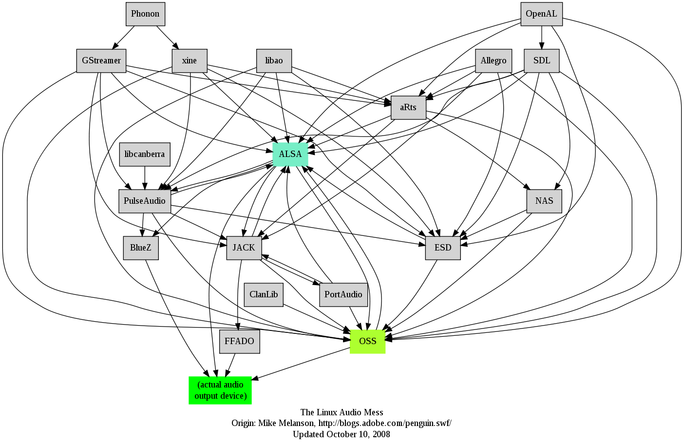
According to TuxRadar [link],
There’s a problem with the state of Linux audio, and it’s not that it doesn’t always work. The issue is that it’s overcomplicated. This soon becomes evident if you sit down with a piece of paper and try to draw the relationships between the technologies involved with taking audio from a music file to your speakers: the diagram soon turns into a plate of knotted spaghetti. This is a failure because there’s nothing intrinsically more complicated about audio than any other technology. It enters your Linux box at one point and leaves at another.
To and audio application, Linux audio provides several audio subsystems through which audio can be channeled: ALSA, PulseAudio, Jackd, OSS and others. An application can use anyone of these subsystems and in fact they do in order to provide wide appeal and compatibility.
Here is a very simplified and high diagram describing the different audio subsystems and their relationship [link]:

And application can literally take any route through the different components in order to arrive at the hardware. An application can use Alsa, routed through Jack and back to Alsa; or it can use PulseAudio to OSS or Alsa all the way. Audio applications such as MPD can use either ALSA, PureAudio or OSS in order to appeal to a wider audience and provide compatibility to new, old and in-between versions and flavors of Linux.
FOCUS ON ALSA
In our quest for bit-perfect audio, A reasonable approach to simplify the audio path is by minimizing the number of components through which the audio stream can possibly travel.
A practical way to do this is to direct the application to use a single audio subsystem. In our case, restricting to ALSA looks like a good option since it is already included in the Debian BBB release. (At least PulseAudio and Jack are are installed when installing MPD)
This site [link] also has a good overview of the different sound subsystems in Linux. A graphical description of ALSA is as follows:

The key message here is that ALSA looks like a “simple” interface between an audio application and the hardware and that there is a Mixer (Sound Mixing) outside the Kernel that CAN can potentially be bypassed. And indeed it can be bypassed:
A sound developer who wishes to output sound in their application can take any of the following routes with ALSA:
- Output using ALSA API directly to ALSA’s Kernel API (when sound mixing is disabled)
- Output using ALSA API to sound mixer, which outputs to ALSA’s Kernel API (when sound mixing is enabled)
- Output using OSS version 3 API directly to ALSA’s Kernel API
- Output using a wrapper API which outputs using any of the above 3 methods
A further simplification is to restrict the use of ALSA through the ALSA API (a more modern API) and avoid using the OSS v3 API (Legacy API). This may not be an issue as modern applications do not have a need to use the older OSS v3 interface.
MPD (MUSIC PLAYER DAEMON)
Since Volumio and RuneAudio are using MPD, It is a good idea to select MPD and figure out how it works. MPD simply runs in the background playing music from its playlist. Client programs communicate with MPD to manipulate playback, the playlist, and the database. [link]
Configuring MPD to use ALSA
The mpd configuration file is at /etc/mpd.conf. (The default configuration for mpd -as installed for debian, uses ALSA.)
The MPD documentation [link] indicates that it is capable of outputting to 15 plugins (ALSA, PulseAudio, OSS, etc). The configuration file allow the selection of the output plugin. Here is the example for selecting ALSA as the output of MPD:
To configure an audio output manually, add an audio_output block to mpd.conf:
audio_output {
    type "alsa"
    name "my ALSA device"
    device "hw:0"
}
Further, the configuration allows us to disable and bypass any mixing/resampling of the audio data. I’ve highlighted in red the important parameters.
The following table lists the audio_output options valid for all plugins:
Additional ALSA specific fields can be added according to this table (ALSA uses libasound)
| Setting | Description |
|---|---|
device NAME |
Sets the device which should be used. This can be any valid ALSA device name. The default value is “default”, which makes libasound choose a device. It is recommended to use a “hw” or “plughw” device, because otherwise, libasound automatically enables “dmix”, which has major disadvantages (fixed sample rate, poor resampler, …).Note: the default device can be set in the ALSA configuration file. The default device can be set to “hw” type and thus bypassing “dmix” the ALSA mixer. |
use_mmap yes|no |
If set to yes, then libasound will try to use memory mapped I/O. Here is an example using this parameter [link]: “yes” # Minor speed improvement, should work with all modern cards |
buffer_time US |
Sets the device’s buffer time in microseconds. Don’t change unless you know what you’re doing. Note: etc/mpd.conf states: MPD Internal Buffering: ****** This setting adjusts the size of internal decoded audio buffering. Changing this may have undesired effects. Don’t change this if you don’t know what you are doing: audio_buffer_size “2048”. ******This setting controls the percentage of the buffer which is filled before beginning to play. Increasing this reduces the chance of audio file skipping at the cost of increased time prior to audio playback: buffer_before_play “10%” |
period_time US |
Sets the device’s period time in microseconds. Don’t change unless you really know what you’re doing. |
auto_resample yes|no |
If set to no, then libasound will not attempt to resample, handing the responsibility over to MPD. It is recommended to let MPD resample (with libsamplerate), because ALSA is quite poor at doing so. |
auto_channels yes|no |
If set to no, then libasound will not attempt to convert between different channel numbers. |
auto_format yes|no |
If set to no, then libasound will not attempt to convert between different sample formats (16 bit, 24 bit, floating point, …). |
dsd_usb yes|no |
If set to yes, then DSD over USB according to the proposed standard by dCS and others is enabled. This wraps DSD samples in fake 24 bit PCM, and is understood by some DSD capable products, but may be harmful to other hardware. Therefore, the default is no and you can enable the option at your own risk. |
Thus in the MPD configuration we can:
- Specify ALSA as output plugin
- Specify that no mixer should be used in audio output plugin
- Specify that no volume adjustment be applied
- Further disable “dmix” the ALSA mixer (#2 may do the same thing. But you never know…)
- Further disable resampling in the output (dmix?)
- Optionally enable DSD over USB
Here is a guide on setting up MPD that will illustrate some of the parameters discussed above [link].
Configuring sample rate converter in MPD
Now that we’ve taken cared of the output plugin configuration, we need to ensure that other MPD plugins do not do sample rater conversion and/or mixing.
MPD can use one of the following sample rate converter:
- Internal (built in into MPD, low overhead, low quality)
- Sox (provided by libsoxr [link])
- Secret Rabbit Code (provided by libsamplerate [link])
Both libsoxr and libsamplerate can be compiled into MPD so they may be already available in the MPD package. After installing the package mpd in Debian/BBB further request for libsamplerate and libsoxr fails to locate these libraries, likely indicating that these have already been compiled into mpd (I am using “mpd” and “MPD” interchangeably).
SRC (libsamplerate) provides a small set of converters to allow quality to be traded off against computation cost. The current best converter provides a signal-to-noise ratio of 145dB with -3dB passband extending from DC to 96% of the theoretical best bandwidth for a given pair of input and output sample rates. [link] -The MPD documentation lists 97 db SNR [link]. Not sure how the two figures are related.
The MPD documentation says:
The setting samplerate_converter controls how MPD shall resample music.
If MPD has been compiled with libsamplerate support, this setting specifies the sample rate converter to use. Possible values can be found in the mpd.conf man page or the libsamplerate documentation. By default, this is setting is disabled.
Possible values:
| Value | Description |
|---|---|
“internal“ |
The internal resampler. Low CPU usage, but very poor quality. |
“soxr very high“ |
Use libsoxr with “Very High Quality” setting. |
“soxr high” or “soxr“ |
Use libsoxr with “High Quality” setting. |
“soxr medium“ |
Use libsoxr with “Medium Quality” setting. |
“soxr low“ |
Use libsoxr with “Low Quality” setting. |
“soxr quick“ |
Use libsoxr with “Quick” setting. |
“Best Sinc Interpolator” or “0“ |
libsamplerate: Band limited sinc interpolation, best quality, 97dB SNR, 96% BW. |
“Medium Sinc Interpolator” or “1“ |
libsamplerate: Band limited sinc interpolation, medium quality, 97dB SNR, 90% BW. |
“Fastest Sinc Interpolator” or “2“ |
libsamplerate: Band limited sinc interpolation, fastest, 97dB SNR, 80% BW. |
“ZOH Sinc Interpolator” or “3“ |
libsamplerate: Zero order hold interpolator, very fast, very poor quality with audible distortions. |
“Linear Interpolator” or “4“ |
libsamplerate: Linear interpolator, very fast, poor quality. |
It appears that there is no “off” setting, so that MPD will always attempt to resample audio in order to match the capabilities of the downstream components. There doesn’t seem to be a way to remove all the resamplers even by removing libsamplerate and libsoxr because there is always the internal resampler of MPD. In the case of the mpd package for debian, it is likely that libsamplerate and libsoxr have been compiled with mpd, so removal is not possible.
It is also reasonable to assume that if the “samplerate_converter” setting is not used in the config file (the default condition), a default sample rate conversion method would be applied.
We already have a way to disable “dmix” in ALSA which defaults to 48KHz, so there is no need for MPD to resample to 48KHz to meet the requirements of dmix. The only remaining sample rate requirement is the capability of the hardware. It is therefore reasonable to assume that if the hardware is capable to supporting the sample rate of the audio file, then no resampling would be performed.
CONFIGURING ALSA
According to these sites [link]. [link]
There are 3 configurations files that are read every time an ALSA device is opened:
- Default configuration file (comes with ALSA and should not be changed): /usr/share/alsa/alsa.conf
- System wide configuration file (optional): /etc/asound.conf
- User configuration file (optional, residing in the users home directory): $HOME/.asoundrc
There is no need to write a configuration file since the default is always present. However, for our purpose we want to ensure that the data is sent to device without any mixing or resampling by ALSA
Recall from the ALSA-specific settings above:
It is recommended to use a “hw” or “plughw” device, because otherwise, libasound automatically enables “dmix”
Type=hw
Thus we wish to define a “hw” device. For our purpose we create a /etc/asound.conf file with the following entry:
pcm.!default {
	type hw
	card 0
}
The exclamation sign causes the previous definition of pcm.default to be overridden (so we don’t have to worry about the default configuration file /usr/share/alsa/alsa.conf).”card 0″ is the audio device we wish to use. It could be “card 1” or other. See below to determine what to use. “type hw” is used as recommended.
If sample rate conversion is needed, we can use the “plug” type
Type=plug
Use the following entry in /etc/asound.conf
pcm.!default {
	type plug
        slave.pcm {
              type hw
	      card 0
        }
}
EXPLORING THE AUDIO COMPONENTS IN DEBIAN/BBB (KNOWN TO ALSA)
I used this guide [link] to explore and identify the different ALSA components in the Debian distribution for BBB
The presence of /proc/asound directory indicates that ALSA is present:
![]()
The file /proc/asound/cards tells you which sound cards are present in the system. Here is BBB without any external devices. It says there is a native sound device.

The file /proc/asound/devices tells you the features of the cards. The native sound device is an audio playback device.

The file /proc/asound/pcm gives us more detail on the “digital audio playback” (PCM). Here we find that the audio device is provided by the HDMI interface.
![]()
The simplest say to identify which cards are installed in the system is to use “aplay -l” [link]. This gives the same info as /proc/asound/cards and /proc/asound/pcm

Further information on the device capabilities can be obtained from the file /proc/asound/card0/pcm0p/sub0/hw_params. It requires that a track is being played. Notice we use “card0” because the card has been identified as “card0”

alsacap
alsacap serves to list the sampling rates, number of channels and sample formats supported by installed sound cards and their ALSA drivers. This helps to find out which parameters do not require resampling (something to be avoided) and to troubleshoot ALSA problems [link]
However, the tool is only available as source so it needs to be compiled. Here is a sample output from here [link]
$ alsacap
*** Scanning for playback devices ***
Card 0, ID `SB', name `HDA ATI SB'
  Device 0, ID `VT1818S Analog', name `VT1818S Analog', 1 subdevices (1 available)
    2..8 channels, sampling rate 44100..192000 Hz
    Sample formats: S16_LE, S32_LE
      Subdevice 0, name `subdevice #0'
  Device 1, ID `VT1818S Digital', name `VT1818S Digital', 1 subdevices (1 available)
    2 channels, sampling rate 44100..192000 Hz
    Sample formats: S16_LE, S32_LE
      Subdevice 0, name `subdevice #0'
ADDING A USB AUDIO DEVICE
Unlike a PC, a reboot is required for the system to detect the presence of a USB audio device.
After connecting a TI PCM270x-based device (USB 1.1)


After connecting DIYINHK XMOS-based device (USB 2.0)


After connecting AMANERO board (USB2.0)


As can be seen, these cards are all automatically recognized by BBB.
ENABLING I2S OUTPUT
diyaudio’s MIERO has developed a driver to enable I2S output in the BBB [link].
It requires that the HDMI output be disabled (since it shares the same lines with Audio I2S). In my installation, the line to disable HDMI is already there as a comment, so I just had to un-comment it and reboot.
With HDMI disabled (and no other device in the USB port) -no sound cards detected:
![]()
Here are the instructions (copied from the site) to download and install the I2S driver for BBB/Debian. You can just copy each line and paste it in the PuTTY windows (paste by clicking the right mouse button.
download and extract driver
wget http://bbb.ieero.com/botic_driver_v3.tar.gz
tar xvzf botic_driver_v3.tar.gz

install driver (assumes official BBB Debian release)
cp -av botic_driver/firmware /lib/
cp -av botic_driver/modules.bbbdebian/* /lib/modules/

update module dependencies
depmod -a

load driver (Needed after every boot)
echo BB-BONE-BOTIC1 > /sys/devices/bone_capemgr.*/slots

There are 3 configurations for the driver
BB-BONE-BOTIC1 - this is for BBB without cape
- onboard clock (48fs rates only)
BB-BONE-BOTIC2
- onboard clock (48fs rates)
- external clock (44k1fs rates)
- external clock switch on UART1_TXD (pin configurable via DT)
BB-BONE-BOTIC3
- external clock (48fs rates)
- external clock (44k1fs rates)
- external clock switch on UART1_TXD (pin configurable via DT)
aplay -l shows the following

The I2S pins are the following:

TESTING WITH APLAY
Rather than testing with MPD which might invoke its resampler by default, we will use aplay (alsa player) which does not have a resampler of its own. It is a lightweight player for alsa.
I compiled a collection of tracks from 44KHz to 384KHz
![]()
Type=hw: bypassing the mixer
The entry in /etc/asound.conf is as follows:
pcm.!default {
	type hw
	card 0
}
Using this configuration requires that the source file matches both the bit depth and sample rate supported by the hardware. For example, if using the BOTIC driver (which enables I2S output) which is set as 32bit device, you cannot play 16bit nor 24bit files. The error message indicates that only “S32_LE” (Signed 32 bit Little Endian) is supported:

Type=plug, enabling the ALSA mixer
The entry in /etc/asound.conf is as follows:
pcm.!default {
	type plug
        slave.pcm {
              type hw
	      card 0
        }
}
The result is that “dmix”, the alsa mixer is invoked. With a reputation of being bad, hopefully it does fine with bit-stuffing (e.g., converting 16 bit to 32 bit by appending zeros)
Testing the BOTIC driver we obtain the following results:
Playing a 44.1KHz file. We expect conversion to 48KHz because the native I2S in BBB only supports 48KHz and its family of sample rates. And indeed, this is what we find. The first screen shows playing the 44K file; the second screen shows the contents of /proc/asound/card0/pcm0p/sub0/hw_params showing that it is outputting 32-bit 48KHz. Thus we see dmix in action, doing sample rate convertion
![]()

Playing a 192KHz. We expect no sample rate conversion as this is natively supported by the BBB, but dmix will convert from 24 bit to 32 bit. Indeed, this is what we find. The first screen shows playing the 192K file; the second screen shows the contents of /proc/asound/card0/pcm0p/sub0/hw_params showing that it is outputting 32-bit 192KHz. We hope that dmix is just bit-stuffing…
![]()

If playing 176KHz, ALSA resamples to 192KHz.
REFERENCES
BEAGLEBONE BLACK: ACCESSING NETWORK SHARE
ACCESSING NETWORK SHARE
I set up a network share by inserting a USB memory stick to the Airport Extreme WiFi router.
- Address of Airport Extreme: 10.0.1.1
- Name of memory stick: MUSIC (later I changed it to MUSICUSB), fat32 formatted
- password for share: XXXX
1- install the “cifs.utils” package with “apt-get install”

2- mount the share with the following command
![]()
- mount -t cifs does the same thing (it invokes mount.cifs)
- “//10.0.1.1/MUSIC” is the share on the Airport Extreme “MUSIC” is the name of the USB Stick inserted in the Apple Airport Extreme router
- “/media/nas” is the mount point. I created the “nas” directory under /media
- “-o” is the options flag
- “username=any” means no user name is needed (as it is set up in the AE)
- “password=XXXX” is the password used to secure the share (as setup in the AE)
- “sec=ntlm” is the password security mode. Without it you’ll get an “error (22): invalid argument”
- More info here [link]
AUTO MOUNTING OF THE SHARE
Here we will use /etc/fstab and mount the share at boot time. The network share is seldom removed, so mounting it during boot is the best option. I use the following line:
![]()
- Here I had changed the name of the USB Memory device to “MUSICUSB”
- This assumes that your network share is always the same name
- More info here: [link]

Latest Comments