Search Results
BUILDING THE DIYINHK ES9018K2M
I have come to the realization that audio diy never ends. There is never the “final” project. There is always tweaking, a new mod, new stuff. Thus I decided to use a cardboard box as an enclosure. Much easier to work with, simple tools would do.
Many would consider a proper enclosure a must for a diy project, but for me this is good enough. Here is a nice looking Lenovo tablet box.

POWER SUPPLY TRANSFORMERS
Three separate transformers were used:
- DAC supply transformer: salvaged from an VCR from the time that linear supplies were still being used. These transformers are very nice, having at least 2 hefty 9V secondaries. The secondaries feed a TPA dual PS which is used as a pre-regulators for the DAC supplies. The two capacitors hanging off the transformer provides DC to an LED (to indicate power 0n/off)
- Analog supply transformer: 15×2 toroidal transformer. (Got it from Twisted Pear Audio)
- Controller transformer: 6V DC salvaged from a wall-type supply, upgraded the smoothing capacitors


Water bottle caps are perfect for the feet.

DAC AND ANALOG SUPPLIES
Used a quad-supply board. This board is designed to provide 4 x 3.3V/5V regulated output. Two supplies receives pre-regulated DC, two supplies receive AC (thus the larger filter capacitors).

Two of the regulators were modified to provide 14.2 V (1.4V+6.4V+6.4V) for the opamp by shorting pins 4 and 5 to GND. They are also configured to provide +/- 14.2V by tying the +output of one of the regulators to GND (I followed what diyinhk did for their dual +/- supply [link])


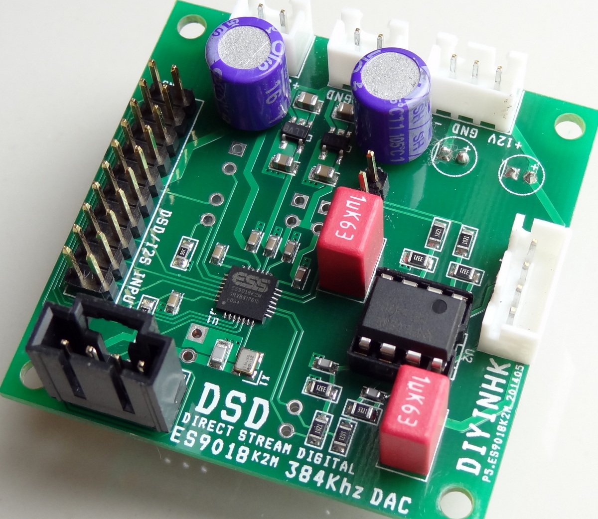
DAC BOARD
Standard build. Only “upgrade” are the electrolytic capacitors. On the backside, the jumpers are to connect the I2C lines to the separate I2C header because I forgot to short the lines on the front side before I soldered the connector (which blocked the jumpers). Later I will upgrade the opamp.

There is a separate SPDIF input connection that feeds the GPIO2 pin in the DAC. Selecting this GPIO pin for SPDIF input has been enabled in the code.
GPIO1 is configured in the board to be in input selection pin for manual selection of I2S/SPDIF. My code does not enable this mode because the selection can be done directly through the user interface. This is here for manual selection with a switch and requires that the chip be programmed in such a way. I believe the diyinhk XMOS interface would program the chip to allow manual selection of SPDIF input.

The board comes with an NDK 80 MHz oscillator [link]. Other implementations may use a 100MHz clock. The software support both 80 MHz and 100 MHz clocks.
In addition, a separate supply can be used to power the clock by cutting the power trace and connecting the supply to the through-hole vias.

ANALOG AND DIGITAL POWER
The external 5V powers a single regulator for the analog 3.3V AVCCR and AVCCL. . The second regulator provides 3.3V to in chip internal oscillator (I think in order to support an external quartz crystal instead of an oscillator). The regulators are marked “LLVB” and are TI LP5907 Ultra Low Noise regulators for analog applications [link]. They rank near the top among ultra low noise regulators [link].
The external 3.3V is used directly without further regulation to power the digital side of the chip and also the local oscillator.

Power to the oscillator is further filtered by a ferrite bead

OPAMP POWER
Positive and negative supply voltage are taken directly to power the opmap.

OUTPUT
The board has connection for the differential outputs straight out of the DAC chip and also single ended output through the opamp. I am using the single ended output wired to a mini-plug for connection to a headphone amplifier. The opamp provided is a NE5532 dual operational amplifier [link]


GROUND PLANE
Nice, solid ground-plane

ALL TOGETHER


Latest Comments