Search Results
AKM Verita 4490EQ DAC
(12/22/14- Updated with information from AKM support engineers -see register section)
It has been a long time semiconductor houses invested in a flagship product. Wolfson announced the WM8471 in 2007 and ESS announced the Sabre DAC in 2008. Recent investment has been concentrated in DACs for the broad consumer industry especially for the mobile segment. It is good to see a company still interested in investing resources for the “audiophile” segment.


AMK introduced the AK4490 this year and has recently made it available in production quantities. It differs upon the AK 4399 DAC in the following areas (yes, the spec for Dynamic Range is lower in the new chip):
| Parameter | AK4490 |
AK4399 |
| THD | -112 dB | -105 dB |
| S/N (Mono) | 123 dB | 126 dB |
| Max Sample Rate | 768KHz | 216 KHz |
| Built-in Digital Filters | 5 | 2 |
| Direct DSD (No conversion to PCM) | Yes | No |
| AVDD Max operating voltage | 7.2V | 5.25V |
Here is an overlay of the FTT measurement between the AK4490 and AK4399 (graph slightly shifted to the right to show the comparison) from the evaluation board data sheets. As seen, the AK4490 has a slight edge over the AK4399:

Increasing S/N by 3 dB
In order to “recover” the lost S/N in the new device as compared with the old device, The AK4490 can be operated with an analog supply of up to 7.2V. At 7V we gain 3dB S/N resulting in 126 dB for mono operation and therefore meeting the best specification of the old A4399 part.
Even though this is not documented in the current version of the AK4490 data sheet, it is documented in the AK4495 data sheet:

Thus one of the “mods” that can be made in this DAC is to run the DAC at the higher-end of the analog voltage operating spectrum.
KEY FEATURES
Built-in Digital Filters
(images taken from Ayre’s paper [link]):
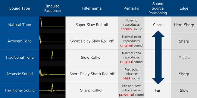
The built-in digital filters consist of 5 selectable filters. They include all the “popular” filters developed so far by different vendors plus one additional filter with undisclosed response (super slow roll-off). The filters are described as follows:
 Linear phase Sharp Roll-off (AKM notation: “no delay”): this is the “standard” sharp roll-off filter found is all DACs. It is also known as the “brickwall” filter. It is said that pre-ringing sounds unnatural.
 Linear phase Slow Roll-off (AKM notation: “no delay”): this is also a “standard” filter found in all DACs. As in the linear phase sharp roll-off filter, it also generates pre-ringing, but trading lower amounts of pre-ringing with letting more aliased image through (theoretically increasing harmonic distortion).
 Minimum delay Sharp Roll-off (AKM notation: “short delay”): this is also called the “minimum phase” or “apodizing” filter that was the rage a few years back. Whereas in the past audio engineers have insisted in phase linearity (meaning all frequencies have equal phase or delay), More recent research have shown that a “minimum phase” filter sacrifices some of the phase linearity (adds some phase distortion) for better time response. This filter removes all the “unnatural” pre-ringing but “dumps” all that energy to post-ringing. Implementation of this filter is also found in the Wolfson WM8741/8742 DACs
 Minimum delay Slow Roll-off (AKM notation: “short delay”): this is a “more modern” type of filter also found in the Wolfson WM8741/8742 DACs. In addition to eliminating pre-ringing, this filter also incorporates slow roll-off and this reduces post ringing as well.
The properties of this filter are similar to the “MP filter” found in Ayres latest CD player.
Super Slow Roll-off: this filter is the differentiating feature (in terms of built-in filters) that this DAC provides. The AKM literature says “super slow roll-off filter with emphasized characteristics” (which really means nothing). There is some information in the marketing page as shown below.
The marketing information says the following [link]
Native DSD Support
Supports 2.8MHz (64fs), 5.6MHz (126fs) and 11.2MHz (256fs) DSD
According to AKM, the volume control module and the delta-sigma modulator can be bypassed for DSD resulting in “direct” DSD rendering. The AK4490 contains an integrated low-pass filter specifically for DSD data. The ultimate specified performance for SACD (as described in the Scarlet Book) can be easily realized with a simple external analog filter.
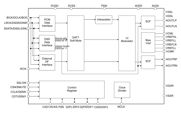
Notice the bypass path for DSD Data. The DSD data is received by the DSD interface and sent directly to the “SCF” (Switched Capacitor Filter) block. DSD filter can be selected at 50KHz, 100KHz or 150KHz cut-off.
Other Comparative Features
Resolution32 bit32 bit32 bit24 bit24 bit
| Parameter | AK4490EQ | ES9018 | ES9018K2M | WM8741 | PCM1794 |
| DR (Mono) | 123 dB | 135 dB | 127 dB | 128 dB | 132 dB |
| THD | -112 dB | -120 dB | -120 dB | -100 dB | -108 dB |
| Max SR | 768KHz | 384KHz | 384KHz | 192KHz | 192KHz |
| Output Mode | Voltage | V or I (best) | V or I (best) | Voltage | Current |
| Resolution | 32 bit | 32 bit | 32 bit | 24 bit | 24 bit |
| DSD Mode | DSD Direct and DSD to PCM | DSD to PCM | DSD to PCM | DSD Direct and DSD to PCM |
Just like the WM8741, the AK4490 supports “direct DSD” processing bypassing the volume control and delta-sigma modulator. And like the WM8741, there is no automatic switching between PCM and DSD.
I2S and DSD shared lines
In order to facilitate the playing of both PCM and DSD content, it is desirable to have the same lines transmit PCM and DSD data. We find that in the AK4490, the I2S and DSD signals are shared. Here is a post I write earlier concerning shared I2S/DSD signal lines: [link]
The table below shows compatible DACs (DACs that share that use the same lines for DSD and PCM) and interfaces showing how the DSD pins are mapped to the PCM/I2S pins:
| I2S Pins |
ESS9018 [link] |
PCM1795 [link] |
AK4399 [link] |
Amanero [link] |
SDTrans [link] |
XMOS Ref [link] |
| BCLK | DSD Clock | DSD Clock | DSD Clock | DSD Clock | DSD Clock | DSD Clock |
| LRCLK | DATA Left | DATA Right | DATA Right | DATA Left | DATA Left | DATA Left |
| DATA | DATA Right | Data Left | Data Left | Data Right | DATA Right | DATA Right |
The AK4490 DAC follows the mapping of the AK4399 which switches channels with the “conventional” channel mapping of USB interfaces. Likely it was the USB interface designers that took notice of the ESS9018 DAC and conformed the channel mapping to that chip.
Fortunately, there is channel remapping in at least the Amanero interface and there is channel remapping in the DAC itself as specified in the following table of the data sheet:

MONO=0, SELLR=1 says:
- Right channel input is mapped to Left channel output
- Left channel input is mapped to Right channel output
DIYINHK IMPLEMENTATION
I Just received diyinhk’s implementation of AKM’s new flagship DAC, the AKM AK4490EQ [link]. This is the first available diy board in the market (that I know of):

POWER SUPPLY LINES
The Diyinhk implementation follows (mostly) the AKM evaluation board and data sheet [link] but maximizes performance whenever possible (like in the selection of capacitor type and value). The board is powered by: 5V line, 3.3V line and +/- 12V line (for the output opamp).

The general layout of the power traces, decoupling capacitors and ground planes also follows the data sheet:
Grounding and Power Supply Decoupling:
To minimize coupling by digital noise, decoupling capacitors should be connected to AVDD and DVDD respectively. VREFHL/R and VDDL/R are supplied from analog supply in system, and AVDD and DVDD are supplied from digital supply in system. Power lines of VREFHL/R and VDDL/R should be distributed separately from the point with low impedance of regulator etc. AVSS, DVSS, VSSL and VSSR must be connected to the same analog ground plane. Decoupling capacitors for high frequency should be placed as near as possible to the supply pin.
Analog 5V supply lines (can operate up to 7.2V according to spec)
The 5V supply connects to VDD (5V Analog supply input) and Reference Voltage High (VREFH) -as recommended in the data sheet.
The differential voltage between VREFH-L/R and VREFL-L/R sets the analog output range. The VREFH-L/R pin is normally connected to VDD (analog 5V supply), and the VREFL-L/R pin is normally connected to VSS1/2/3 (analog ground). VREFH-L/R and VREFL-L/R should be connected with a 0.1µF ceramic capacitor as near as possible to the pin to eliminate the effects of high frequency noise…All signals, especially clocks, should be kept away from the VREFH-L/R and VREFL-L/R pins in order to avoid unwanted noise coupling into the AK4490.
In addition, according to the eval board manual, a large value capacitor between VREFH-L/R (Analog 5v) and VREFL-L/R (GND) improves the THD performance in accordance to the following graph:
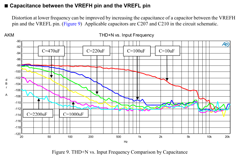

The Diyinhk board is implemented with 2200 uF capacitors, achieving the best THD numbers. (The larger capacitor holds the reverence voltage stable -perhaps an even larger capacitor would further improve the low frequency THD numbers).
There is an option to use separate supplies for right and left VREF and VDD. This also follows the scheme implemented in the official evaluation board where the left VREF is separately powered from the right VREF.

Further, the AKM literature states:
Special designs techniques for sound quality are applied to each blocks for achieving balanced, smooth and powerful signal flow. In addition to L/R perfectly symmetrical layout, more than 5x trace width is used for signal line compared existing products, supplying rich current to analog signal output blocks. To achieve low impedance, two analog power supply pins and two signal reference pins are assigned for each channel, allowing the system to utilize thick PCB trace pattern giving low impedance sources.
The board takes advantage of this feature to use thicker lines for VREF and VDD
All 0.1 uF decoupling ceramic capacitors are C0G

The official evaluation board has a provision to separate the VREF from the Analog 5V VDD which is not implemented in this board. However, it is easy to mod and use separate supplies for VREF and Analog 5V VDD.
The evaluation board implements VREF with the following circuit:

3.3 V Supply Line (Analog 3.3V and Digital 3.3V)
There is a 3.3V analog supply pin and a 3.3V digital supply pin in the chip. The default implementation of the diyinhk board uses the same supply line but filters them with a ferrite bead. By removing the ferrite bead, the user can use separate supplies for the analog and digital 3.3V.

In the evaluation board, AVDD and DVDD are powered by separate regulators:


GROUND PLANE
The ground planes follows the recommended separation between analog and digital sides (along pins 17-18 and 45-46)


SOFTWARE INTERFACE
The older device, the AK4399 supported a 3-wire serial interface. This seemed a not too widely supported protocol (it was not SPI and could not find a similar protocol in Arduino libraries , but one could code the protocol “by hand” as it was just a serial protocol -never tried it though)
Fortunately the new DAC supports I2C protocol (and maintains support for the original 3-wire serial interface found in older DACs). This greatly facilitating the interface to a microcontroller such as Arduino because of their built-in support for more standard protocols such as I2C and SPI.
The advantage of using the S/W interface is that it supports features such as volume control and DSD which are not available through the H/W interface.
The following table summarizes these features that are available in H/W interface (parallel interface -by pulling hardware pins up or down) and S/W interface (serial interface -microcontroller control).

Not indicated in the table is the “super slow roll-off” filter which is enabled by a register setting in s/w mode.
REGISTER DEFINITION SUMMARY
(Updated with information from AKM support engineer)
Here I summarize the register settings and the different functions that can be programmed. I also attempt to do some “translating” of AKM’s vocabulary to more “traditional” vocabulary.
I was able to communicate with AKM to clarify the functionality of certain sections.
Register address: 00 (Control 1)
 7 6 5 4 3 2 1 0
|_|_|_|_|_|_|_|x| Reset chip without initializing registers
|_|_|_|_|x|x|x|_| Interface mode: 16bit, 24bit, 32bit, I2S, LJ... (1)
|_|_|x|_|_|_|_|_| External digital filter clock: 768KHz/384KHz
|_|x|_|_|_|_|_|_| Enable/disable external digital filter mode
|x|_|_|_|_|_|_|_| Master Clock frequency Setting: auto/manual (2)(3)

NOTES:
(1)- The only requirement for bitclock is >= 2x bit depth. Bitclock could be
32fs, 48fs or 64fs. Not limited to always be 64fs as in ESS DACs
(2)- Auto: detects master clock frequency and sampling frequency (44.1KHz,
96KHz, ...) automatically; sets oversampling rate (1x, 2x, 4x...) according to
input MCKL (this is kind of obvious).
Note: AKM calls sample rate "sampling speed" and assigns names to typical
sample rates: 44-48KHz="normal", 88-96KHz="double", 175-192KHz="quad"...
(3)- Manual: manually set the sampling rate (44.1KHz, 96KHz...) Use reg 01 and
reg 05 for sampling rate setting. This means, in its simplest form, manually
matching the sampling rate to the incoming data sample rate to use the highest
oversampling rate allowed by the system and thus obtain best noise performance.
This feature can also be used to select a different sampling rate (typically a
lower oversampling rate); for example, if selecting "normal" for 44.1KHz allows
8x oversampling (512fs), selecting "double" results in 4x oversampling (256fs).
This allows for experimentation with different oversampling rates and can be
used to tailor the sound for those inclined to lower oversampling or even no
oversampling. The use of lower oversampling results in higher noise for these
kind of DACs. AKM indicates in the datasheet that using a lower oversampling
rate (512fs to 256fs) results in a decrease of S/N of 3dB.

Register address: 01 (Control 2)
 7 6 5 4 3 2 1 0
|_|_|_|_|_|_|_|x| Mute/unmute
|_|_|_|_|_|x|x|_| De-emphasis: Off, 32KHz, 44.1KHz, 48KHz
|_|_|_|x|x|_|_|_| Manual setting of sampling speed: "normal", "double"... (1)
|_|_|x|_|_|_|_|_| Short Delay/Traditional filter (Minimum/Linear phase)
|_|x|_|_|_|_|_|_| Zero data detect mode: Separate channels or ANDed channels
|x|_|_|_|_|_|_|_| Zero data detect ON/OFF

NOTES:
(1)- Manual sampling speed setting uses 3 bits. The third bit is in reg 05.
See notes on register 00 for additional info on manual settings

Register address: 02 (Control 3)
 7 6 5 4 3 2 1 0
|_|_|_|_|_|_|_|x| Filter cutoff slope: fast/slow
|_|_|_|_|_|_|x|_| MONO mode: left/right
|_|_|_|_|_|x|_|_| Invert output pin level on zero detect
|_|_|_|_|x|_|_|_| MONO/STEREO mode
|_|_|_|x|_|_|_|_| DSD Data on clock falling/rising edge
|_|x|_|_|_|_|_|_| DSD master clock frequency:512KHz/768KHz
|x|_|_|_|_|_|_|_| PCM/DSD mode

Register address: 03 (Left Channel Attenuation)
 7 6 5 4 3 2 1 0
|x|x|x|x|x|x|x|x| Attenuation (1)
NOTES:
(1)- 256 levels, 0.5 dB each. 00=mute; ff=max volume

Register address: 04 (Right Channel Attenuation)
 7 6 5 4 3 2 1 0
|x|x|x|x|x|x|x|x| Attenuation (1)
NOTES:
(1)- 256 levels, 0.5 dB each. 00= mute; ff= max volume

Register address: 05 (Control 4)
 7 6 5 4 3 2 1 0
|_|_|_|_|_|_|_|x| Super Slow filter on/off
|_|_|_|_|_|_|x|_| Bit 3 of the manual sampling speed setting (see reg 01)
|_|x|_|_|_|_|_|_| Left channel phase invert ON/OFF
|x|_|_|_|_|_|_|_| Right channel phase invert ON/OFF

Register address: 06 (control 5)
 7 6 5 4 3 2 1 0
|_|_|_|_|_|_|_|x| DSD bit 0 of sampling speed selection (bit 1 is in reg 9)(1)
|_|_|_|_|_|_|x|_| DSD Mode: Direct/Convert to PCM (2)
|_|_|_|_|x|_|_|_| DSD Automute release when Automute release is in "hold"
|_|_|_|x|_|_|_|_| Automute release: Auto/hold (3)
|_|_|x|_|_|_|_|_| Right Channel DSD flag when detecting full scale signal
|_|x|_|_|_|_|_|_| Left Channel DSD flag when detecting full scale signal
|x|_|_|_|_|_|_|_| DSD AutoMute: ON/OFF (4)

NOTES:
(1)- There is no facility for setting auto sample rate detection for DSD. The
use must detect the incoming DSD sample speed and match the sampling speed.
Will have to experiment to see what is the effect of sample speed mismatch.
(2)- In DSD direct mode, the volume control and delta-sigma modulator are
bypassed. In PCM mode, it converts to PCM and uses volume control block and
delta-sigma modulator. DSD direct with a combination of the internal filter
and simple output filter meets the filter specification of the SACD Scarlet
Book.
(3)- Automute condition disappears when data becomes under full scale
(4)- Automute condition is when data is full scale

Register address: 07 (Control 6)
 7 6 5 4 3 2 1 0
|_|_|_|_|_|_|_|x| Synchronize ON/OFF (1)

NOTES:
(1) Synchronizes multiple DACs when used together in the same system. Read
data sheet for more information.

Register address: 08 (Control 7)
 7 6 5 4 3 2 1 0
|_|_|_|_|_|_|x|x| Sound Quality Control Setting (1)

NOTES:
(1): Sound Control has 3 settings: "1", "2", "3". The AK4495 data sheet shows
additional settings "4" and "5". These setting refer to the 5 different filters
that are available in the DAC. They serve the same function as the filter
selection bits specified in the other registers. What is unclear is which
register takes precedence.

Register address: 09 (Control 8)
 7 6 5 4 3 2 1 0
|_|_|_|_|_|_|_|x| DSD bit 1 of sample speed selection (see also reg 5)
|_|_|_|_|_|_|x|_| DSD filter selection when in DSD direct mode

Latest Comments