Archive
Firmware v 0.99
The long awaited firmware update for the Soekris DAC is out.
| Parameter |
Firmware 0.9 |
Firmware 0.99 [link] [link] |
| Digital Filters FIR1 Coefficient Size and Format | FIR1: 32 bit, 2.30 format
FIR2: 32 bit, 2.30 format |
FIR1: 32 bit, 1.31 format (one bit of increased precision).
Should be good down to around -150 db. Increased precision improves frequency response (pass band ripple and stop band attenuation) [link] -One extra bit of precision adds 6 db improvement. FIR2 format remains the same. |
| Digital Filters FIR1 Number of Coefficients | 1016 max coefficients | Twice the number of coefficients resulting in 2032 max coefficients. Basically anything possible with software resampler (such as SOX) will be possible in the DAC. |
| Digital Filters FIR1 and FIR2 Filter selection | A single filter per supported sample rate. Changing filters requires uploading the new filters through the serial interface. To switch to the new filters a power cycle, input switch or sample rate change is required. | 4 banks or FIR1 and corresponding FIR2 filters per supported sample rate can be individually selected. (FIR1 filters specified as type 4-7 corresponding to banks 1-4 and FIR2 filters specified as type 8-11 corresponding to banks 1-4). NOTE: For simplicity in creating filters: if a specific FIR1/FIR2 filters are only specified once for bank 1 (FIR1 type 4 and FIR2 type 8), then they are used for the other banks e.g.: [link]
The factory filters are: Linear, Mixed, Minimum and Soft. As before, new filters can be uploaded replacing the factory filters. Example filter configuration: [link] A filter bank can be selected by selecting the FIR1 type (4-7) or name given to the filter. The corresponding FIR2 filter in the bank is automatically selected. A power cycle, input switch or sample rate change is first required when uploading new set of filters. |
| De-emphasis Filter | “Original” | “Improved”. Note: de-emphasis filters are always loaded, but only enabled when emphasis bit is set in spdif datastream [link]. If a CD is ripped, then the emphasis bit is lost. It is up to the ripping s/w to detect the emphasis bit and apply de-emphasis when ripping. Apparently only iTunes can do this automatically: [link], [link] |
| Digital volume control | -99 dB to 0 dB | -80 dB to 10 dB with zero crossing detect (to eliminate glitches during volume level transitions). Also fixed the polarity inversion bug [link], [link] |
| Locking to incoming data bitclock and wordclock | > 1 sec (up to 2-3 sec). This happens when the incoming bitclock and/or wordclock is interrupted or changes frequency when changing tracks | < 0.2 sec, near instantaneous. Locking pops [link] initially present in the first release of the new firmware have also been fixed (same version number) |
| Interrupt-driven Serial Port | No | Yes. This prevents loosing characters at high speed (prevents the DAC from loosing characters when a computer or microprocessor sends commands to the DAC at high speed) |
| Input selection | Auto, SPDIF 1, SPDIF 2, I2S (although it does not quite work) | Same: Auto, SPDIF 1, SPDIF 2, I2S (bugs fixed) |
| Isolated 3.3V Serial ports | Not enabled | Enabled. Can be used to interface to uP like Arduino or Raspberry Pi for external s/w control without having to use a serial to RS232 converter device [link] |
| Output Mode | Stereo only | Normal Stereo, Inverted Stereo, Mono Left, Mono Right. In Mono, the raw output is also in balanced mode.
For multiple boards, the plan is “to daisy chain the serial ports, the echo of all commands should make it possible. Then use volume pot and input selector on the first one in the chain… Paralleling the I2S and Toslink inputs are easy, SPDIF might require buffering…” However, perhaps a better solution is to use separate serial ports to control each board (if for only setting one board MONO Left and the other MONO Right). An Arduino Mega or DUE has multiple serial ports. |
| Activate newly uploaded firmware or filters | Power cycle | In uManager, after download type “update” and then type “exit” to exit the uManager (and return to “play” mode). “update” should only be used to update the firmware because it erases and rewrites the uC internal flash which is a high risk process. [link]. I believe power cycle will do the same thing (but didn’t try) |
NOTES
- Input rate of 352.8K or 384K will result in FIR1 being bypassed [link]
- uManager settings (filter, volume, etc) are stored in flash and survive power cycling. This is used to setup power-on default settings.
- In uManger, “set filter =…” should be “set filters = …”
Updates to Firmware:
1.05 filters are the same as 0.99 filters, only added support for DSD rates which require their own filter definitions. The filter files are interchangeable, but for DSD to work you of course need the DSD filters….
1.05 had bugs which in certain circumstances could cause the dam1021 uC to lock up, that should be fixed in 1.06. Any other versions was test versions and should be gone by now…. [link]
COMMAND INTERFACE
| Area | Play-mode Command interface |
Setting Command interface (uManager) |
Comments |
| Best Usage | Microprocessor Control | Setting power-on defaults, interactive control | Settings with uManager are saved to flash and survive power cycle. Note the use of capital letters when using “play-mode” interface |
| Input Selection | Ix | set input = x | x=0: I2S Input
x=1: SPDIF 1 (typically coax) x=2: SPDIF 2 (typically toslink) x=3: auto. It locks to the first detected active input in the order I0, I1, I2 |
| Volume Control | Vxx | set volume = xx | Sets volume to xx level in dB. xx = -80 to +10 |
| V-99 | set volume = -99 | Enables potentiometer volume control. NOTE: If set to other than -99 and the potentiometer is connected, the DAC may be MUTED (having no output whatsoever and unresponsive to the volume pot) -at least this was the behavior in the older firmware. | |
| Show Filters | N/A | filters [all] | Show current selected filter (“filters”). Show all possible filters (“filters all”) |
| Switching filter bank | Fx | set filters = “name” | Select filter bank with immediate effect. Both FIR1 and FIR2 filters in the bank are selected. [link].
x=4-7 representing filter banks 1, 2, 3 and 4. “name” is “linear”, “mixed”, “minimum”, and “soft” are are mapped to filter banks 1, 2, 3 and 4 regardless of what type of filters you have in those banks. [link]. Note: although “set filters” can be used to select filters, is meant for setting the default filter. At power up, the DAC is always at the default filter |
| Other Commnads | N/A | See –> | Enter/Exit uManager: “+++” to enter; “exit” to exit
Set serial communication speed: “conspeed=xxx“. I think only use if having problems with the highest speed: 115200 Set mono/stereo: “mode=x“. x=”normal”, “invert”, “bal-right”, “bal-left”: Normal STEREO, Inverted STEREO, MONO Left, MONO Right. In MONO, the raw output is also in balanced mode. Update firmware (not to be used when uploading new filters): “update“. NOTE: “update” should only be used to update the firmware because it erases and rewrites the uC internal flash which is a high risk process. |
UPLOADING THE NEW FIRMWARE
Summary of steps:
Connect DAC RS232 port to RS232 port in PC
- Start the terminal application and configure the serial port parameters
- Enter DAC uManager by typing “+++”
- Type “download” and use the terminal application Xmodem transfer facility to upload file
- Type “update”, then acknowledge update with “y” (yes) – Caution: Don’t use “udpate” when just uploading filters
- Type “exit”
Connect the RS232 Interface to a PC
Since this is the first time the isolated serial ports have been enabled, the existing firmware in the DAC can only communicate via the RS232 ports.
Connect the RS232 pins to the PC serial port as follows. This is basically a null-modem connection without h/w flow control. You may want to check this informative site on serial communications including RS232 [link]
Launch the Terminal Application
I use “Tera Term” [link]. The latest version is 4.87 and it works well with Windows 10. A mini tutorial can be found here [link].
Select “Serial” connection upon startup of the application. Configure the serial communication parameters with the following settings by selecting “Serial port” in the “Setup” menu:
- Baud rate: 115,200 (This is pretty fast. Use a good, short cable)
- Data bits: 8
- Stop bits: 1
- Parity: none
- Flow control: none

Invoking “uManager”
- Type “+++”
Wait for the DAC to respond (~1 sec). You will see the following message:

Uploading the new firmware
- Type “download” in the terminal window.
uManager will respond with “Start sending file using XMODEM/CRC protocol” and wait for you to start the xmodem transfer.
- In the terminal application “File” pull down menu select “Transfer” -> “Xmodem” -> “Send” from the File menu. Select the file and click “Open”.

Transfer will start immediately:

- Type “update” and then “y” to the prompt “uManager Firmware Update, are you sure?”
- CAUTION: Some users have reported that “update” when just updating filters have bricked the DAC. This is because “The update command should only be used when loading new firmware, it erases and rewrites the uC internal flash which is a high risk process, and if something goes wrong it would require hardware to fix it” [link]

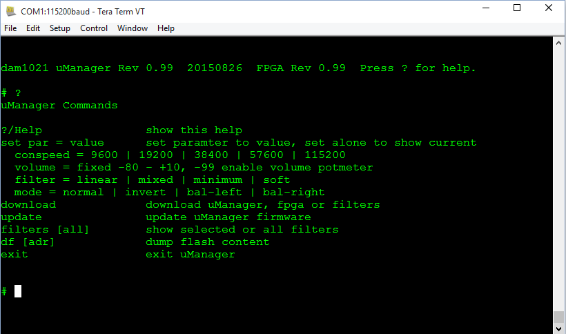
Comparison between uManager 0.8 and 0.99:
RELOADING FIRMWARE IN A BRICKED DAC
Our friend Paul has details on reloading the firmware without uManager (in case you crash/corrupt the firmware and can’t get uManager to work) [link], [link]
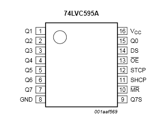
The firmware resides on the onboard microprocessor which is is the STM32F030 uC [link].
The pin out of the microprocessor is the following (from datasheet [link])
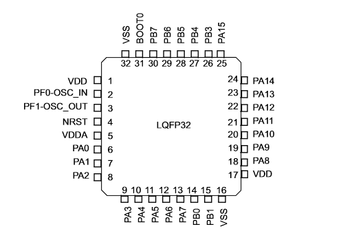
Programming is through the “SWD” pins (from application note AN4325 [link]):

PA13 and PA14 are pins 23 and 24 (lower left corner of the chip)

If you follow the traces, you can see where they are connected in J4:
Requirements:
- Get a hold of a ST-LINK/V2. [link] This is a programmer for STM32 (the microprocessor in the DAC board)
- Download ST-LINK utility [link] and user’s manual
- Email Soren and ask for a copy of the uManger firmware (also available from Paul’s website -the link above)
Connecting programmer to DAC board
The Pin definition of the ST-LINK is as follows (from user guide [link]):
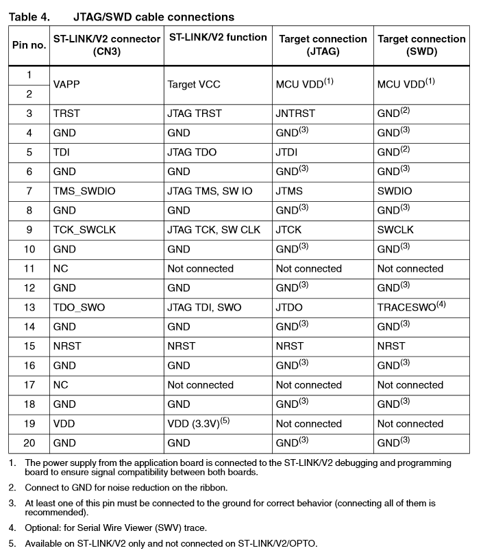
Since the target connection is SWD, we look at the last column and determine that only 5 pins need to be connected:
- Pin 1 or 2: MCU VDD (the VDD of the microprocessor – requires that the DAC board be powered on -also see Note 1 in the table above)
- Pin 20 (0r any GND): GND
- Pin 7: SWDIO
- Pin 9: SWCLK
- NRST (Reset) -This is pin 4 of the microprocessor, not sure if connected to J4

Flashing the firmware
- Select “Erase Chip” to erase the flash in the microprocessor to ensure clean flashing
- Select “Program” or “Program and Verify” and select the uManger bin file (Section 3.5 of the manual)

Soekris DAC: Modding VRef
MUST DO MOD?
As it turned out, the implementation of the 4V reference voltage in the Soekris DAC has been found to be sub-optimal. Fortunately, thanks to experiments and measurements by industrious individuals of the audio diy community, Soren, the designer of the DAC, has reviewed the design and has proposed an official “factory” mod which is fairly easy to do.
Thus this “mod” seems to be a “must do” in order to achieve the intended designed performance of the DAC, but to many that have been already satisfied with the sonic signature of the DAC, this mod would definitely improve the enjoyment department.
4V (and -4V) REFERENCE
Shift Registers
In the Soekris DAC, there are 16 LVC595A shift registers (chip markings indicate that it is an NXP LVC595A [link]).

The diagram below depicts the pin description. We are interested in finding out how Vref is related to the shift register.
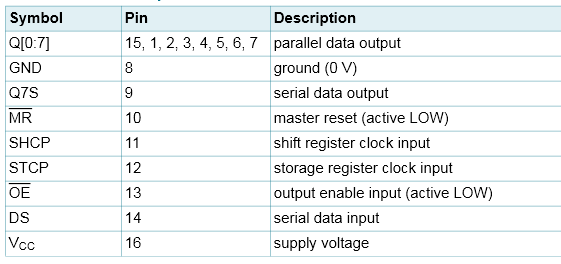
A shift register outputs will be either VLow (0V) or VHigh (VCC) in accordance to the serial data input and clock. Q0 to Q7 are the outputs of the device.
According to these posts [link], [link], the shift registers provide the voltage source to the resistor ladder. These devices “drive” the resistor ladder to convert the digital signal into an analog signal. In order to further understand this concept, lets look at the basic configuration for an R-2R DAC network show below:
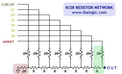
For this 8-bit example, D0 – D7 are the 8-bit digital value to be converted to an analog output and can have two values: VLow, representing the digital value “0”); and VHigh, representing the digital value “1”. In a typical implementation, VLow = 0V and VHigh = Reference Voltage
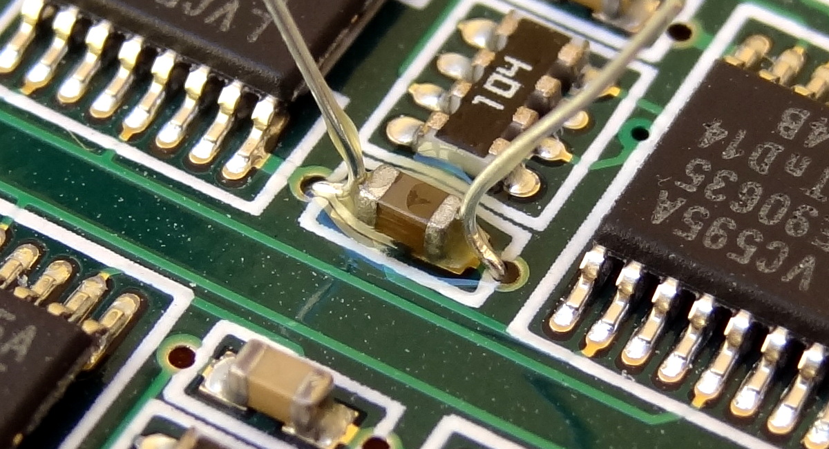
It can be seen from the circuit diagram that for a “0” input (VLow), the output is “0” and for a “1” input (VHigh) the output will be some fraction of the Reference Voltage determined by the equivalent resistor divider connected to that particular input. In the Soekris DAC, the outputs of the shift registers are connected to the inputs of the resistor ladder as shown in the following photo:

We can therefore see that the reference voltage is the VCC of the shift register. It follows that in the Soekris DAC the quality of the VCC is perhaps the single most important factor affecting the quality of the output signal because this voltage is directly applied to the resistors in the ladder.
Improving Vref
In most DACs, the quality of Vref is directly related to the quality of the output signal. In terms of measurements, this is expressed in the THD numbers.
As an example, the datasheet of the new AKM 4490Q DAC, shows that improvements to the Vref can be accomplished by adding capacitance to that pin. The datasheet shows a THD measurement diagram with increasing values of capacitance applied reference voltage pin:
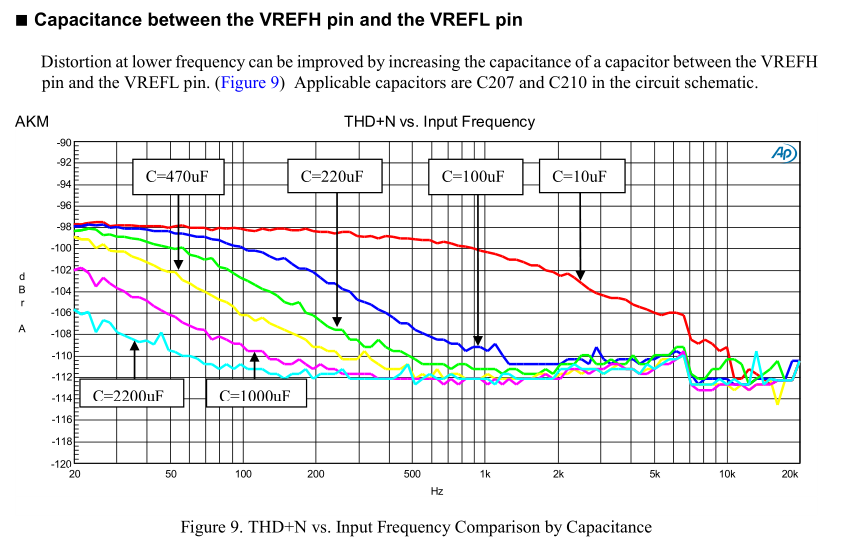
Notice that continuous improvement to the THD performance is obtained with increasing capacitance. Even if using more than 2200 uF.
It follows that one can safely assume that increased performance in the Soekris DAC can be had by using large value capacitors to bypass the reference voltage.
Indeed, power supply mods and experiments shared by “alecm” at the diyaudio forum shows both audible and measured improvements when Vref is bypassed with a large size capacitor. In fact, “alecm” showed that the reference voltage is far from clean and that it exhibits a fairly large ripple modulated by the input signal [link]. The maximum ripple was measured at 6mV (0.15% out of 4V). We can see that this is 3X the deviation contributed by the lowest grade resistors which is 0.05%
The following traces (borrowed from the diyaudio forum post) show the before and after mod comparison of the reference voltage Vref.
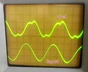

In the words (paraphrased) of alecm, the mods provided:
- Deeper soundstage
- Greatly increased dynamics
- Increase in resolution and details
Implementing the mod
To facilitate modding, Soren provided the location of the output capacitors for the +/- 4V references and their polarity markings [link]:

Soren has also provided some recommendations [link]:
- The Vref buffer design are unconditional stable with large capacitance, so you can hang on as much as you want, but 220uF to 470 uF low ESR / polymer on each of the four Vref supplies is a good choice.
- It’s unnecessary to add multiple smaller capacitors as the PCB have power planes with smaller ceramics at each ‘595 shift registers
- You can also get 47uF X5R 6V3 ceramics in 0805 size, easy to stack on top of existing capacitors….
- Please don’t try external Vref supplies, they’re not needed and the risk to ruin your board is great.
Because Vref has been designed to be stable with “as much capacitance as you like”, I will implement this mod by adding capacitors at each VCC pin in order to increase the capacitance and also for the fun of it.
If we follow the polarity of the +4Vref and of the -4Vref to each shift registers, we find the following:
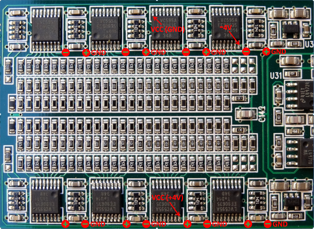
Notice that for the bottom row, the VCC pin of the shift register is connected to +4Vref, and this is where I will install the larger capacitor. In the upper row, the VCC pin of the shift register is connected to GND. Assuming a solid ground pin, there is no need to install a capacitor here. Instead, the ground pin of the shift register is connected to the -4Vref. Here I will install the larger capacitor. The photo above shows one channel of the board. The other channel is built exactly the same.
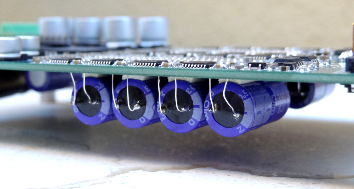
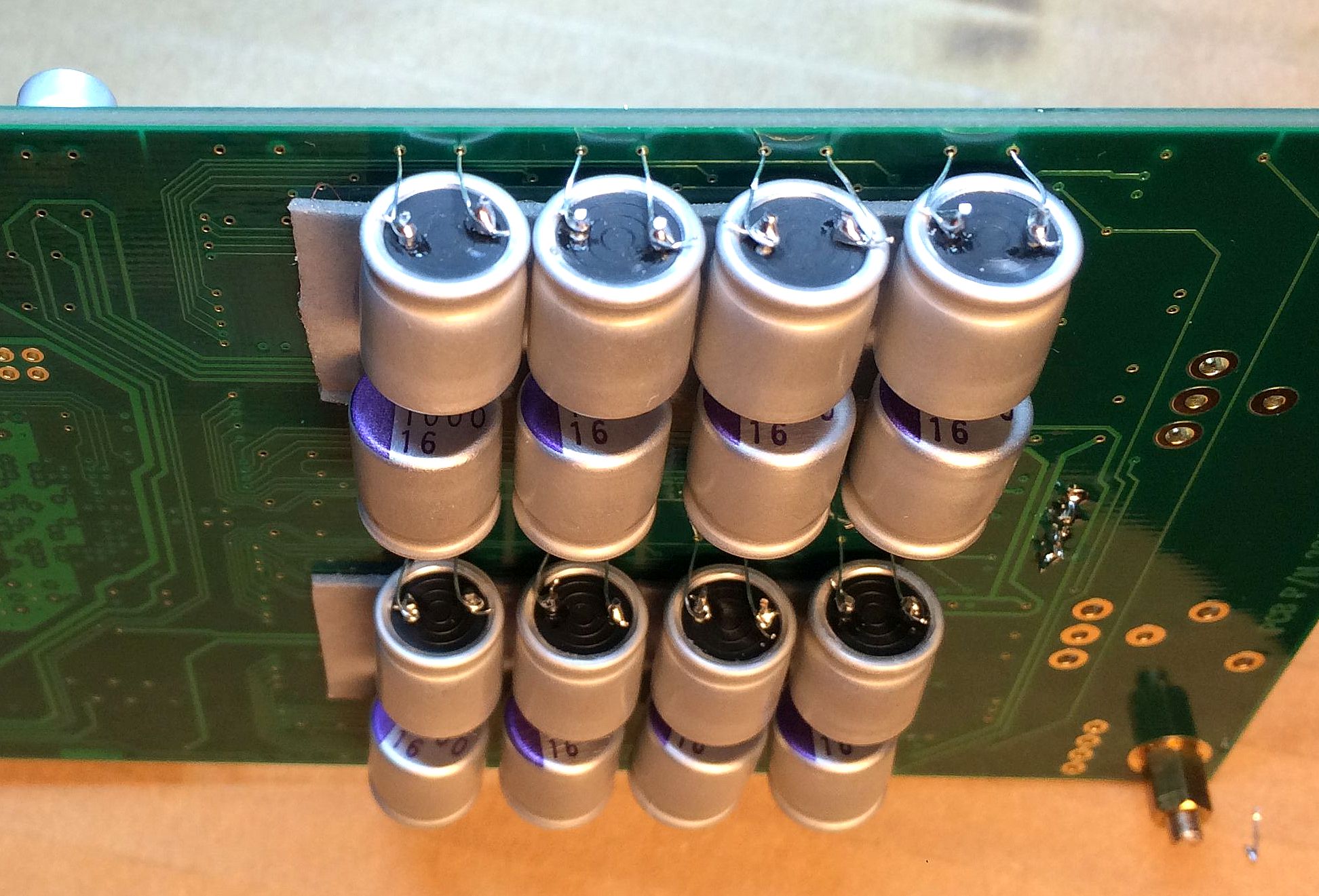
I have a number of 330 uF, 6.3V OSCONs that I picked up from industrial surplus. These have the leads cut (I think) for automated board stuffing. To solder them to the VCC capacitors, I need to extend their leads. More on the OSCONs here [link]

TIP: In the past I had piggybacked electrolytic capacitors on top of the ceramic capacitors and with just a slight bump to the electrolytic, you can inadvertently detach the ceramic capacitor from the board [link] -so you must be extra careful if using this method.
The extension wires are thin enough to fit through the power and GND vias. This way I can glue the capacitors to the back side of the board and bring the leads to the front side through the vias. I used some thin insulated wire (after stripping the insulation). I don’t know what gauge but they fit both the small vias (output capacitor of Vref buffer) and large vias (shift register’s VCC capacitor). You can also use the single strands from stranded wiring.

I used double stick tape to glue the capacitor to the backside of the board. You can also use a hot glue gun to affix the capacitors.

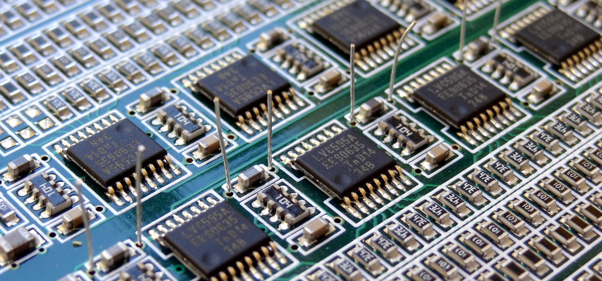
Bending the wires closer and in contact with the ceramic capacitor to facilitate soldering. Actually I measured continuity and the wires already make contact through the vias. I don’t think it is possible to solder the wires to just the vias, surface tension and solder mask may prevent good flow and contact.

Add flux (this is a must to allow the solder to quickly flow to the intended location):
And carefully solder the wires to the ceramic capacitors (practice with an old board if you are new to soldering SMD devices). Thin gauge leaded solder works best. There maybe some appeal for lead-free or silver loaded solder but those are harder to work with – not compatible with amateurs like us. Just wash your hands well afterwards 🙂


To get professional results, I use Isopropyl alcohol (rubbing alcohol) with an old toothbrush to clean up the flux afterwards.

Here are the 8 capacitors for the +4V reference:

All together:
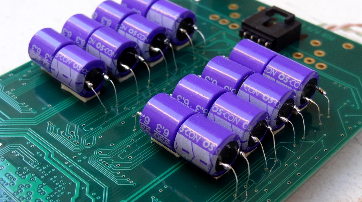
Beautiful!
Note that this is the “best” we can do with a capacitor mod to “clean up” the reference voltage. Whatever we do to ensure a clean reference voltage is limited to what happens inside the shift register. A shift register is designed and specified to switch between two voltages: a high voltage corresponding to “one” and a low voltage corresponding to “zero”. They are also designed to meet a minimum switching speed, but the outputs are not specified to meet a precise voltage, but rather just a minimum voltage for VHigh and a maximum voltage for VLow. It is amazing that this DAC works so well given the fact that it is implemented with shift registers.
The OSCON capacitors I used are old stuff. The company ended manufacturing of those models in 2011. New technology uses solid conductive polymer (rather than Organic Semiconducting Polymer -where the name OSCON comes from).
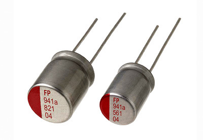
Newer capacitors have even better performance with respect to low ESR and are very inexpensive. For example the following Nichicon FPCAP R7 Solid Polymer [link] at $0.50 in quantity 10 for a 16V 330 uF, ESR=7 mOhm.
Here is a comparison of FPCAP with conventional electrolytic capacitors

UPDATE: Circuit Simulation
Our friend Filter-Meister Paul has simulated the 16-cap mod (in fact this exact mod) and has shared his results in a 3-part post [parit1] [parit2] [parit3]
The result shows the expected peaking:

Further improvements can be obtained by (comments section of part3):
Stock+1000uF has a fairly big noise gain peak around 3.67KHz. With the load oscillating at that frequency the ripple is 3.595mV. If the load is oscillating at 1KHz ripple is 0.169mV. It will basically follow the same trajectory as the Stock+470uF plot with a lower peak frequency.
Factory Mod +1000uF the sim’d ripple at 1KHz is 1.006mV, while at 3.67KHz it’s 0.510mV. The worst case with the FactMod+1000uF is 1.226mV at 100Hz, which is about 1/3rd the worst case ripple of stock+1000uF.
If you wanted to tweak a bit, try replacing the 0.1R resistor with a 0.01R. There will be a very small amount of peaking above 10KHz but using the 0.01R should cut the ripple quite significantly.
UPDATE: FACTORY FULL MOD
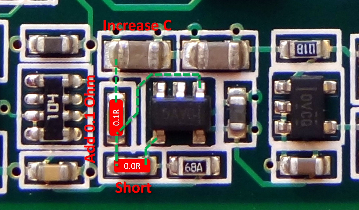
Soren published the official recommendation for modding for Vref [link]:
- The output capacitor of the buffer, can be paralleled (increased) as much as desired, but a single 47uF X5R 0603 capacitor is sufficient and will fit nicely on the board. (Original value is 22 uF)
- The output series resistor needs to be much lower in the order of 0.1 ohm and it is used to eliminate a small peak at the output. This can be done by adding a 0.1 ohm resistor in parallel with the existing 10 ohm resistor. A 0.1 ohm 0603 SMD resistor would fit nicely. (Original value 10 ohm)
- The feedback capacitor is to be removed from the feedback loop by shorting it with a wire or with a 0.1 ohm 0603 SMD resistor [link]. A short can also be used here as indicated by the Soekris: “You can use shorts for the feedback capacitor, but since you already would have to source those 0.1 ohm 0603 resistors it’s easier to use those as shorts…” [link]. (Original value 330 pF)
The result in less than 1 mV p-p ripple independent of frequency; with no peaks or changes in voltage precision. It is also what the next production series will look like.
Happy about #1. This is the same as the capacitor mod I have done and good thing that increasing the capacitance as much as desired is OK. I didn’t want to remove some of the capacitors I put in as the mod looks real cool :-).
Recent measurements [link] have shown that the performance (ripple reduction) of this mod can be further improved by adding more capacitance beyond the the recommended 47uF. Glad to know my implementation of the mod is not just for looks :-).
Update [link]: Vref differences between the different versions
- Original rev1: 10R series resistors, 22 uF output capacitor, 330 pF feedback capacitor and 499R feedback resistor
- Factory upgraded rev1 and production rev2: 0.1R series resistor, 47 uF output capacitor, 499R resistors mounted in both capacitor and feedback resistor position (this gives a 998R feedback resistor), creating an effective 0.050R vref buffer output impedance.
- Production rev3: 0.1R series resistor, 47 uF + 3x 100 uF output capacitors, 1K00 resistor mounted in feedback capacitor position (orange), 301R resistor mounted in feedback resistor position (yellow), creating an effective 0.025R vref buffer output impedance.
Colors on attached drawing:
- Red: Output capacitor.
- Blue: Series Resistor.
- Orange: Feedback capacitor (now used for resistors).
- Yellow: Feedback resistor.

Advantages of this mod
I can think of the following additional advantages of this mod over the recommended factory mod:
- Smaller effective ESR by paralleling several capacitors
- The VCC pin of the shift register is the 0ptimal location for the added capacitor (even though the solid power plane allows installing the capacitor away from the VCC pin)
- For multiple capacitor installation, this is the best “mechanical” approach. It would be hard to mount multiple capacitors at the location of the buffer output capacitor.
For #2, this requires ordering resistors from one of the part shops. Not a common size to find in recycled boards. Got to put a larger order. Not worth paying shipping for a few SMD resistors. Maybe there will be more improvements from the diyaudio community. I’ll wait a little while on this one.
For #3, a wire short will do. This makes a buffer a simple voltage follower. I think this would be easier to do than soldering the 0.1 ohm SMD resistor: bend the wire in U shape, put some solder on the ends and reheat the solder when placed in contact with the ends of the capacitor. This will have to wait for #2
Is #1 alone good enough?
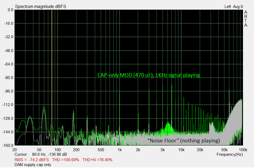
More measurements shared at diyaudio [link] shows the results of different mod iterations. In particular, the stock buffer with 1000 uF of output capacitance compares favorably with the factory mod with 1000 uF. In fact, except for a “bump” at around 4KHz, it has lower noise in frequencies below ~3KHz. Thus the question: is adding 1000 uF to the stock buffer good enough?
I over-imposed several traces to compare the the mods in question:

In this graph, the stock+1000uF is ~20 dB lower noise in the 1 KHz component than the factory mod+1000 uF. Only the components beyond the 3rd harmonic (4KHz and beyond) are slightly higher.

Another set of measurements show a similar result [link]. I believe this mode refers to this cap configuration [link]. The results are pretty similar to the adding of capacitance to the stock buffer’s output capacitor. Notice the “bump”.
Further measurements [link] shows that by increasing the added capacitance from 1000uF to 2700 uF on the stock buffer, the bump is totally eliminated:
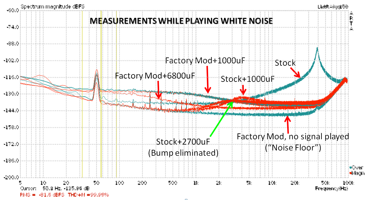
Looks like I will leave my mod (which is just adding capacitance to the stock buffer configuration) as-is for the time being. I’ll see what further results can be had from further experimentation.
Update [link]
Soren offers these options for VREF mod:
There are basically two way to good result:
1- The official modification with 0.1 ohms resistors and 47uF capacitors, all smt parts which can be a little tricky to solder…. Afterwards, you can add additional large capacitors, any type. But I admit that soldering 0603 smt parts are not that easy, so:
2- Just add large enough electrolytic capacitors without changing the smt parts, simulations show the best result with 3300 uf low impedance electrolytic on each rail, just your regular good caps, you don’t want their impedance to get too low, 40 mOhm is perfect for the 3300 uF.
There are an additional internal power supply impedance in each LVC595 shift registers, I have measure 0.3 ohm. That mean that there is really no reason to get the vref impedance insanely low….
JUST THE BEGINNING FOR VREF?
I think effectively, this mod brings the reference voltage implementation to the same level as the initial factory recommendation from ESS for the Sabre DAC and implemented in the BI DAC[link]:
The implementation of the critical analog supply, the AVCC, was as recommended in the ESS application note [link] with DVCC is used as a reference to the regulating opamp. This configuration provided a low impedance supply to the analog pins [link]. But he main drawback was the pretty nonexistent PSRR (power supply rejection ratio), so the PSRR of the analog supply was pretty much the PSRR of the DVCC that was used as the reference [link].


So maybe there are more improvements to be made.
However, there are unique challenges in the Soekris DAC to consider: the Vref needs to be of dual polarity and track each other. Another thing to consider is the question of how accurate the reference needs to be when the resistors cannot be more accurate than 0.01%. Further, there are also inaccuracies to the voltage applied to the resistor ladder introduced by the shift registers. So perhaps the current design is optimal at this point in the sense there are no performance bottlenecks nor performance overkill anywhere in the circuit.
FURTHER READING
Check out Filter-Meister Paul’s blog [link]
Another 16-cap implementation [link]

Yet another [link]


One more [link]
R2R DAC Benchmark Filters (for now)
After a 5 month long, 1200-post filter development odyssey [link], our friend Paul have arrived at a set of benchmark filters for the enjoyment of all owners of the Soekris DAC (BIG THANKS!). There is so much material and knowledge in the diyaudio forum thread that it was a challenge to keep up with. Fortunately, Paul will be moving to a blog format to share new filters, but likely after new firmware for the Soekris DAC is released.
I have summarized the latest “benchmark” filters here for convenience.
| Filter File Name |
Type |
Description |
| 1021filtNQ_C960_140 [link] | Nyquist filter “approaching NOS” | Further “tweaking” of the Nyquist filters, less coloured than the C128 series filters. |
| 1021filtNQ_C960_140dp [link] | Nyquist filter “approaching NOS” | Same but quantized in mkrom.exe. (rather than in MATLAB) (sound far more open in the top end and less clouded) |
| 1021filtNQ_C128_100bp [link] | Nyquist filter “approaching NOS” | The “benchmark” filter with correct “quantization”. Use this one instead.The .txt files here [link]Comparison 128 vs 960 here [link], [link]Response comparison with NOS [link] |
| 1021filt_384_C130_MP [link] | Minimum Phase | Further experimentation with minimum phase. This filter is similar in length and roll-off to the stock 44.1 filter, but minimum phase. It is -0.1dB at around 19kHz. Trading “Nyquist” with minimum phase. Notation: 384 = number of taps; C = Chebyshev Window; 130dB = Window side lobe attenuation setting; MP = minimum phase or LP = linear phase.One of the key determining factors is impulse response [link]. Here is the impulse response for the latest favorite filters: [link] |
| 1021filt_SoX_fixup_HiAtt [link], | High Stop Band Attenuation |
|
| 1021filt_1015_Kb16_BW [link] | High Stop Band Attenuation | After a long road, this filter and the previous one are the current “best” filters.
|
| 1021filtNewNOS [link] | NOS | And for convenience sake, the NOS filter remains a favorite.Latest iteration of the NOS filter which includes POS’s improved de-emphasis filter.”The NOS filter does not actually filter at all – all the coefficients are set to 1 so the audio is passed unaltered and is only up-sampled. The side effect is none of the mirror images of the original signal that appear in the up sampled signal are removed…””Listened to NQtb65, NQtb70 (see Nyquist filters below) and NewNOS today. All three are pretty nice. But NewNOS feels distinctively more dynamic, direct and more full-bodied…” |
| 1021filt_EQHQ_V2r1 [link] | “Perfectionist”(Brick Wall) | I call this “Perfectionist” because it is a “best specification” filter: minimum band pass ripple, high stop band attenuation, narrow transition band…- 0.0000003dB pass band ripple constraint – all filters
|
NEW FIRMWARE (JUST SOME DETAILS)
The new firmware will provide the following enhancements for filter development [link]:
2.30 format for FIR filters was chosen to have reserve, thinking there was plenty of bits, especially when compared to other DAC chips, and 1016 taps were also more than any DAC chips. But after following Paul’s fantastic filter work it seems like that improvements are needed to the filter blocks, even as they already are better than any DAC chip.
As the R-2R DAC should be state of the art, I will change format in next firmware rev, probably to 1.34, and instead have the mkrom tool check for overflow, maybe even look into auto scaling…
I’m also looking into double the number of coefficients, that would require to assign double the MAC blocks to the first FIR filter, should be possible as the last MAC block is just doing volume control, that can be done using a multiplier built with a lot of LUT’s instead, not an issue as that don’t need to be fast and there are plenty of LUT’s left in the FPGA, the FPGA was choosen more for number of MAC blocks than number of LUT’s…
This means
- Increase in coefficient precision (4 additional bits)
- Increase in the number of coefficients (up to 2032 coefficients). Basically anything possible with software resamplers (such as SOX) will be possible in the DAC.
UPLOADING FILTERS
Up to now, I have been using the factory filters. It is time to upload and try some of these filters. For convenience, I am repeating here information from other posts.
Connect the RS232 Interface to a PC
Connect the RS232 pins to the PC serial port as follows. This is basically a null-modem connection without h/w flow control. You may want to check this informative site on serial communications including RS232 [link]

Launch the Terminal Application (Tera Term) [link]
After launching Tera Term (the application is “ttermpro”), select “Serial” and select the Port you are using to communicate with the DAC.

Configure the serial communication parameters with:
- Baud rate: 115,200 (This is pretty fast. Use a good, short cable)
- Data bits: 8
- Stop bits: 1
- Parity: none
- Flow control: none
Click on the “Setup” pull-down menu and select “Serial port”

Invoking “uManager” for Interactive Mode
Type “+++” and wait for the DAC to respond (~1 sec). You must enter “+++”, otherwise there will be no response. If you enter anything else, there will also be no response. “+++” invokes the “uManager” enabling interactive communication with the DAC through a terminal window. You will see the following prompt:

Uploading the filters
After invoking the uManager, type “download” in the terminal window. The DAC will acknowledge your command and wait for you to start the xmodem transfer

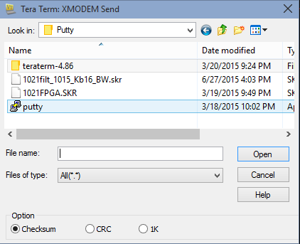
In the “File” pull down menu select “Transfer” -> “Xmodem” -> “Send”. You will see the XMODEM send dialog box (shown below). Select the filter file you wish to upload (in this example “1021filt_1015_Kb16_BW.skr” and click “Open”. Make sure the file is of type .skr.
After completion, power-cycle the DAC. Note: changing the input or changing a track with a different sample rate also triggers reloading of the filters
MY OTHER POSTS ON THIS DAC
| TITLE | SUBJECT |
LINK |
DESCRIPTION |
| Soekris dam 1021 R-2R DAC ILLUSTRATED GUIDE | Users Manual | [link] | Users manual for the Soekris DAC. |
| Soekris dam1021 Build | Build Guide | [link] | Details of my initial build of the Soekris DAC. |
| dam1021 R-2R DAC MODs | Mods | [link] | Mods I have performed on the DAC build. |
| dam1021 R2R More Mods | Mods | [link] | Later mods on the DAC build. |
| Digital Filters for Soekris R2R DAC | Digital Filters | [link] | Extensive list of DIY filters from the diyaudio filter brewing forum thread. |
| R2R Benchmark Filters (for now) | Digital Filters | [link] | Latest set of filters developed and shared in the diyaudio filter brewing forum thread. The best filters of the bunch. |
| R-2R DAC For The REST of US | Technical Details | [link] | Introductory post describing the innovations and capabilities implemented in this DAC. |
| The Soekris R-2R DAC: Technical Details | Technical Details | [link] | Additional technical details of the Soekris DAC that were not covered in the post above and collected after I had the DAC on my hands. |
dam 1021 R2R More Mods…
UPGRADING THE POWER SUPPLY
I Have been pretty happy with my current implementation of the Soekris DAC, using a basic “workhorse” 7812/7912 based power supply. These are legendary for their ruggedness and still the most widely used regulator family for most commercial HiFi equipment.
But not having a lot of time and/or patience to try different mods, I mainly rely on good engineering and the collective wisdom of the people at the diyaudio forums. And lately, improvements in sound have been reported using low noise supplies with the Soekris DAC board [link].
In addition, there is always the attraction for “new and improved” and the introduction of low cost, low-noise supplies in recent years makes upgrading an almost a “must do” thing for diy people like us 🙂
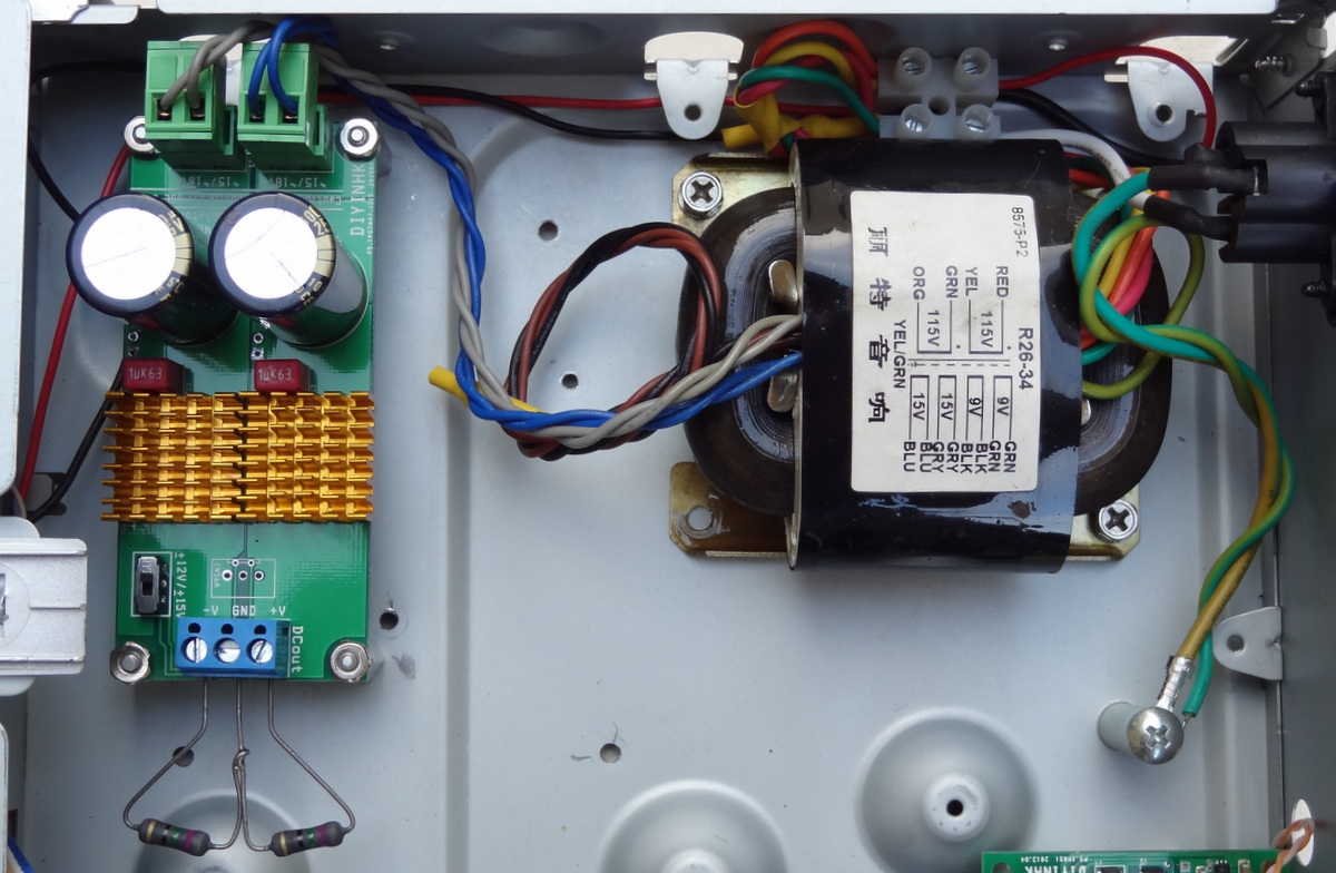
I decided to upgrade the power supply section with a TPS7A47 based power supply kit from diyinhk and an R-core transformer. The TPS regulator has very low noise and a wide operating range. The R-core transformer has multiple (4) secondaries that can feed multiple supplies.
Some users are using shunt regulators for this board. But with the local regulators being of the series type, I don’t think the benefits of a shunt regulator (very low impedance, with “instantaneous” power delivery) can be realized. (Besides I would need to build from bare PCBs and that would take a long time).
Before:

After:

The diyinhk kits are based on the factory recommended PCB layout and as shown in the evaluation boards. As such they should perform as specified in the datasheet.
The kits implement some enhancements over the evaluation board such as built-in AC rectification, large filter capacitors, heatsinks, screw connectors and noise-reducing film capacitor. I am using the +/- 12v-15v bipolar supply kit.
The bipolar supply uses TPS7A47 regulators for both the positive rail and the negative rail. I had inquired diyinhk why not use the TPS7A33 [link] for the negative rail and they replied saying that the chip was very frail and had destroyed a few during prototyping. These kits have been available for a while, implying that they in fact work well.

The transformer has 4 secondaries. I can add two more supplies later… These transformers have the following specs:
- Primary : 0-115vx2,
- Secondaries : 0-9X2(0.7A),0-15X2(0.7A)

What is so good about R-Core transformers?
Here is an excellent resource comparing the different types of transformers [link]. I have summarized here the main advantages of the R-Core:
| Parameter | R-Core |
Toroidal | EI |
| Leakage flux | The Balanced winding cancels the leakage flux. The total amount of leakage flux is extremely small. (1/10th compared to EI) | The winding is not balanced hence there is lot of leakage flux. | There are gaps in the magnetic path and the winding is not balanced resulting in very high leakage flux. Requiring shielding. |
| Efficiency | Very low losses result in better efficiency. Efficiency > 90%. | Efficiency is better than EI transformer but less than R-core transformer. | More losses result in poor efficiency. |
| Exciting Current | Exciting current is minimal as magnetic paths align with the rolling direction of the steel. Also gapless core | Less than that in EI transformer, but higher than that of R-core due to lack of balancing of winding. | Higher exciting current is required due to presence of magnetic gaps, the inability to use the effect of rolling direction of grain oriented steel, etc. |
| Heat generation | Heat generation is minimal due to low Iron loss. The large surface area of the coil allows for better heat dissipation. | The core is not exposed at any point. Thus the heat generated has no area for dissipation. | Due to iron loss the heat generation is more. Large part of the winding is covered inside the core resulting in poor heat dissipation. |
| Size | 40% smaller than EI transformers |
I first tested the supply with two 75 ohm resistors (at 12v this results in 160 mA of current -which is approximately the current consumption of the DAC board). It is always a good idea to test everything while building the circuit. This will prevent frying some component (or even frying yourself). Always exercise caution when dealing with line voltages.
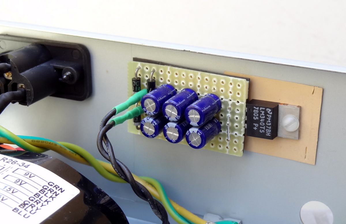
5V Auxiliary supply (for the “dirty” side of the isolators)
HEAD AMP
I have been using the on-board output buffer connected directly to high-impedance headphones (Senn HD-580, rated at 300 ohm). The output buffer, the LME49724 [link] is specified to drive a load as small as 600 ohms while meeting specifications. At 300 ohm, it should be pretty close to spec.

Using the Philips Fidelio X1 (with a measured impedance of 37 ohm [link]), the direct connection seemed less pleasant (than the Senn headphone). Thus the need for a “real” head amp or at least a buffer with sufficient driving capability.
The diyinhk D1X is an inexpensive head amp implemented with a couple of LME49610 high performance audio buffers.


The kit comes with “basic” dual opamps. I had some OPA627s which I obtained when they first appeared in the market, and used those instead.

Due to the size of the dual chip carriers, some of the capacitors had to be installed on the back side.

I mounted it on the back of the case (because there is already a hole for the plug).

Direct connection to the DAC’s raw outputs:
RUNNING TOO HOT…
After hooking up the power supply to the DAC Board and head-amp, the temperature at the heatsink of the power supply was running up to 75C and this is with the case cover off. Although likely a “safe” operating temperature since the specified maximum junction temperature is 125C, this is way too hot for my liking. In addition, with the cover on, it will be heating everything inside the case which will make run even hotter. Regardless of whether it can run at this temperature at extended periods of time, it is just not good practice running your parts are this high temperature.
The 15V outputs of the transformer measured about 18V AC (This results in about 25V DC). This means that with the TPA, being a low drop out regulator, approximately 12V is applied across the regulator itself. With a 12 V output, the amount of power dissipated by the regulator is just as large as the power dissipated by the DAC board – no wonder it gets so hot.
Actually, this would be a very good transformer for a Salas Shunt implementation. From the manual of the Salas, it specifies:
Voltage drop across regulator: Get a transformer that for DC gives you at least 5V extra from your target voltage. 7-10V is better against mains fluctuations, transformer regulation with high current etc.
But the TPA regulators which is a low drop out regulator only requires about .3 V of headroom and 12 V extra is totally unnecessary.

I therefore used a different transformer, this one has 2X 9V AC secondaries and a primary specified to run at 220V. According to the label, each 9V output can supply 0.85A which is plenty for our application (30VA total power).
I rewired it for 120V operation (I don’t remember exactly what I did, but likely I changed the series input connection into parallel connection). The measured output was almost 12V AC loaded. Perfect.


Now running at 35C… Perfect!

ELIMINATING RINGING IN TRANSFORMER SECONDARIES
The correct way is to use a properly designed snubber, but the second best and much easier to do is to use a small value capacitor across the secondary [link]
The ringing is caused by the parasitics of the transformer + rectifier circuit. The parasitic inductance of the transformer windings and routing set up a resonant circuit with the stray capacitance of the circuit. When the current in this resonant circuit is interrupted, as when the diodes turn off, the energy left in the resonant circuit will cause it to ring until the energy has been dissipated in the parasitic resistance of the circuit. The ringing tends to be in the 100s of kHz to low MHz range – so well outside the audio band.
…
There are several ways to address this ringing. One can add a small capacitor (100 nF is usually a good starting point) across each secondary winding. This lowers the frequency of the ringing and effectively suppresses any coupling into the amplifier.
100 nF film caps across the secondaries:

I also added a capacitor across the primary:
NO MORE POPS
(At least with headphones)
In addition to several enhancements over the original D1 headamp, the D1X implements an output signal relay:
The new distinctive feature is our customized power on delay and instant off output relay circuit. It can prevent the annoying power on/off clicks and pops, and with the DC servo circuit, expensive headphones are further protected from damage.
Especially for this DAC, this feature comes as a real bonus. The incredibly loud POPs during power on/off are totally eliminated.
MY OTHER POSTS ON THIS DAC
| TITLE | SUBJECT |
LINK |
DESCRIPTION |
| Soekris dam 1021 R-2R DAC ILLUSTRATED GUIDE | Users Manual | [link] | Users manual for the Soekris DAC. |
| Soekris dam1021 Build | Build Guide | [link] | Details of my initial build of the Soekris DAC. |
| dam1021 R-2R DAC MODs | Mods | [link] | Mods I have performed on the DAC build. |
| dam1021 R2R More Mods | Mods | [link] | Later mods on the DAC build. |
| Digital Filters for Soekris R2R DAC | Digital Filters | [link] | Extensive list of DIY filters from the diyaudio filter brewing forum thread. |
| R2R Benchmark Filters (for now) | Digital Filters | [link] | Latest set of filters developed and shared in the diyaudio filter brewing forum thread. The best filters of the bunch. |
| R-2R DAC For The REST of US | Technical Details | [link] | Introductory post describing the innovations and capabilities implemented in this DAC. |
| The Soekris R-2R DAC: Technical Details | Technical Details | [link] | Additional technical details of the Soekris DAC that were not covered in the post above and collected after I had the DAC on my hands. |
Digital Filters for Soekris R-2R DAC
(Update 5/9/15)
Great news from Soekris on enhancing the filter capabilities of the DAC [link]:
Original coefficient resolution:
The format used in the FPGA of the dam1021 it’s 2.30 fixed point format for the FIR filters and 3.29 fixed point format for IIR filters. (2 bits for the integer part, 30 bit for the fractional part =32 bits). The mkrom utility (part of the filter tools) reads and process the input .txt parameter files as 64 bit floats, including the multiplier, then convert to the 2.30/3.29 fixed formats in the final step, which are pretty good.
Using full 35bit for coefficient resolution in next version or firmware:
Numeric format will probably change to 1.34, and instead have the mkrom tool check for overflow, maybe even look into auto scaling…
Number of filter taps in next version of firmware: 2032 taps (Original, 1016 taps)
I’m also looking into double the number of coefficients, that would require to assign double the MAC blocks to the first FIR filter, should be possible as the last MAC block is just doing volume control, that can be done using a multiplier built with a lot of LUT’s instead, not an issue as that don’t need to be fast and there are plenty of LUT’s left in the FPGA, the FPGA was choosen more for number of MAC blocks than number of LUT’s…
DIY DIGITAL FILTERS
Upload it yourself
Up to now there has been some attempt in allowing custom digital filters to be uploaded or programmed into a DAC. As an example, the ESS DACs allow the user to program filter coefficients into the internal registers of the DAC through its I2C interface.
I had attempted to do so by carefully following the specification and instructions in the ESS data sheet, but was unable to succeed and after many tries I eventually gave up. Some have claimed success, but no one has shared any information to the audio diy community as to how to make loadable custom filters work. Perhaps there is some information that is not public; perhaps I am not smart enough to do so.
With the Soekris R-2R DAC, custom loadable filters has finally become a practical reality. Practical in the sense that finally “any one” can do this.
Filters that you can distinctly hear
User selectable filters has been available for quite some in DAC boards and CD players. With the Wolfson 8741 a user could choose among five filters, including an “Apodizing” and “Minimum Phase” filters what were all the rage a few years back. The ESS DACs allows the user to select among 3 filters and the better DACs have a collection of filters to select from.
If one peruse the forums for listening experiences involving the Wolfson or ESS DACs, there is not much to say about these filters. At most user reports show very subtle differences between the filters and most of the listening impression reports omit specifying the filter that is being used. When I put together a WM8741 (Twistedpear Audio) a few years back, I spent some time listening to the 5 different filters without detecting much differences.
The listening experiences shared at the diyaudio filter brewing threat shows for the first time (at least to me) clearly discernible digital filters. There could be several explanation for this:
- Manufacturers attempt to maximize measured performance with their filters whereas the Soekris filters are the result of experimentation and evaluation-by-ear. In some cases, the “best sounding -or most likable” filters are NOS or near NOS which measure the worse.
- Manufacturers filters are “short” vs longer filters in the Soekris DAC. This allows more experimentation and fine-tuning. As an example, the Soekris DAC filters can have up 1016 coefficients in FIR1 and up to 120 coefficients in FIR2. In contrast the ESS 9018 DAC allows programming 64 coefficients in FIR1 and 16 coefficients in FIR2.
- There could be some placebo effect too. Now that everyone can manipulate filter coefficients, everyone can hear big differences between the filters
There could be more reasons, but users are having a lot of fun with the diy filters for the Soekris DAC.
[“Disclaimer”: I am still using the factory filters. I am afraid of filter overload and want to wait for the “ultimate” filter :-)]
The filter brewing thread at diyadio [link] is pretty extensive and documents the learning experience of a few individuals. It is a “conversation” among these few individuals and a few brave early experimenters sharing their listening impression.
In an attempt to capture the knowledge from that thread, I have summarized the collection of filters by our friend Paul [link]. A few filters are developed by other users, but the overwhelming majority are from Paul. Instrumental to diy filters is also the free tool “rePhase” [link]. I can’t capture all the knowledge that has been shared (due to my own lack of knowledge) but I think it is a pretty good summary.
Up to today, there seem to have been 3 stages of filter development arriving at a (temporal) benchmark filter.
FIRST STAGE: NOS sounds good…
The first state is mostly imitating the response curves from filters available in commercial DACs. For example the filters from Ayre and the filters from Cambridge DACMagic. This was the stage to get comfortable with the creation tools, the curve plotting tools, the specifications and format of the filters and acquiring general knowledge on digital reconstruction filters. Looking at the different filters created, it seems that the experimentation was kind of random.
Out of this stage, the most notable filter is the NOS filter: 1021filtNewNOS and the filter modeled after the DacMagic: CRaPMagic_LP
| Filter File Name |
Type |
Description |
| 1021filt [link] | Linear Phase, “Standard” Sharp roll-off | This is the original dam1021 factory filter. Actually it is rather “medium sharp”: around -17dB down at 22kHz, and doesn’t fully attenuate until 24kHz [link] |
| 1021filt_FIR2_MP [link] | Same as factory filter above but with different FIR2 | The FIR2 filter has been replaced with minimum phase slow roll-0ff [link] |
| 1021MinPhase-Slowrev1 [link] | Minimum Phase, slow roll-off | Inspired by Ayre’s “Minimum Phase Listen” filter. No pre-ringing, small post-ringing. Ayre’s white paper here [link] |
| 1021LPSRO441 [link] | Linear Phase, slow roll-off | Inspired by Ayre’s “Linear Phase Listen” filter. Minimized pre and post ringing |
| 1021SA1 [link] | Linear Phase Apodizing (slow roll-off starting at 10KHz, -100db at 21KHz) | Inspired by Craven’s Apodizing filter but in linear phase. Minimum pre, post ringing and minimum aliasing, but soft on the top-end because of the much earlier roll-off. Apodizing filters were the rave a few years back |
| 1021SA2F2v1 [link] | Linear Phase Apodizing (slow roll-off starting at ~12KHz, -100db at 22.5KHz) | Same as above but starting roll-off at a higher frequency but still way before 20KHz. Maybe good for old people 🙂 |
| 1021filtPOS [link] | Minimum Phase, sharp roll-off. No pre-ringing, but lots of post-ringing | By POS (creator of rePhase) [link]. “Standard” minimum phase filter. |
| MB2b [link] | Linear Phase, sharp roll-off, using Taylor windowing algorithm, 2x oversampling | MB2b is the same as MB2 [link] but with 2x oversampling [link]. It was used in a shootout with other high-end DACs [link] -very interesting read and well written. dam1021 came out second. |
| DAC 44,1kHz-brickwall [link] | Linear Phase, sharp roll-off. Lots and lots of ringing, pre and post. “Standard” filter. | By POS. Possibly equal to the original filters. But this is in rePhase format. Use this as a learning tool to create the filter coefficients and then use Soren’s tool to convert to binary formal for uploading to DAC. |
| 1021filtNewNOS [link] | NOS (Since there can only be one NOS filter, this is the only one to use) | Latest iteration of the NOS filter which includes POS’s improved de-emphasis filter.”The NOS filter does not actually filter at all – all the coefficients are set to 1 so the audio is passed unaltered and is only up-sampled. The side effect is none of the mirror images of the original signal that appear in the up sampled signal are removed…””Listened to NQtb65, NQtb70 (see Nyquist filters below) and NewNOS today. All three are pretty nice. But NewNOS feels distinctively more dynamic, direct and more full-bodied…” |
| 1021filt_35HR_LP [link] | Linear Phase, sharp roll-off, FIR2 has 3.8 dB attenuation (this is totalcrap v1) | Another brick-wall filter with lots of pre and post ringing, with a 3.8 dB attenuation in FIR2 to prevent clipping and benefit those not using digital volume control |
| totalCRaP_rev2 [link] | Same as V1 above, but FIR2 is (linear?) slow roll-off | Experimenting with changing FIR2 filters. The TC filters are actually sharper than the original factory filters. More ringing than factory. [link] |
| CRaPMagic_LP [link] | Linear Phase, Slow roll-off (-8dB at 22KHz) | Modeled after DacMagic Linear setting. Check user manual for filter behavior: [link]. I think this has similar behavior as Ayre’s Linear Phase “listen” filter. This filter also has a MP slow roll-off FIR2 [link] |
| 1021filt_Mix-Phase1 [link] | Mixed phase. Near minimum phase, slow roll-off, minimum ringing | Inspired by Ayre’s MP filter |
| A_CRaP_take on_BH [link] | Intermediate Phase, 80 dB Stop Band Attenuation (tradeoff between ringing and aliasing) | Inspired by John Swenson/Bottlehead:“The intermediate phase splits the difference and has a small amount of pre ringing and post ringing that is a little bit longer than linear phase but much less than minimum phase. This is also deliberately a short filter”.[link] |
SECOND STAGE: Intermediate Phase is good too…
During the second stage of filter brewing, our friend Paul focused (I think) in reducing ringing and in particular pre-ringing by using slow roll-off response and intermediate phase (a combination of liner and minimum phase). The realization at the end of the experiments is that the length of the transition band (the rolling off part) and the amount of phase mixing has a lot to do with how we perceive sound. Small changes in the size of the transition band and small changes in the amount of phase mixing can result in substantial improvements.
Based on the results, there seem to be a lot of experimenting left since there are 3 variables that can be changed: start of roll-off, size of transition band, and amount of phase mixing.
Out of this stage, the most notable filters are the 1021filtIPv4_p30 and 1021filtIPv4_p35 filters.
| Filter File Name |
Type |
Description |
| 1021filt_DTYWS [link] | Linear, “medium sharp” roll-off. (For old people) | DTYWS (“Damn Those Young WhipperSnappers”). Is a filter that has been customized to “old people” that can’t hear past 16KHz. It starts to roll-off at just under 16kHz, is down a comparatively restrained 22dB at 20kHz, is -130dB at 22kHz and bottoms out at -180dB at 22.4kHz. It’s only -0.02dB at 17kHz, then -0.8dB at 18kHz, -6dB at 19kHz, and -21.5dB at 20kHz. Measurements here [link] |
| 1021filtIPv1 1021filtIPv2 1021filtIPv3 [link] | 3 Intermediate Phase filters slow roll off, with different size transition bands and -6dB point. Stop band starts around 25-26kHz so there will be some imaging. (Also for old people) | V1: roll-off starts at 16KHz and has a transition band of 10,000 Hz. -6dB is at 20.0KHz. “Sounds a little bit too soft in the top end. Cotton wool wrapped, and lacking in detail”. V2: roll-off starts at 17KHz, transition band is 9,500 Hz. -6dB is at 20.5KHz. “Increasing the -6dB point by 500hz, and narrowing the transition band by 500hz removes most of the cotton wool effect”.V3: roll-off starts at 17KHz, transition band is 9,000 Hz, -6dB is at 20.75KHz. |
| 1021filtIPv4_p25 [link] 1021filtIPv4_p30 and 1021filtIPv4_p35 [link] | Intermediate Phase with p=25 (p=0 is minimum phase, p=100 is linear phase). Starts rolling off much later than above filters | V4: -0.1dB at 19kHz, -10dB at 22050hz. fully attenuated at just over 26kHz. Has new linear FIR2 which is now flat out past 40kHz and attenuates below 300kHz.. .txt files here: [link](These filters are a favorite among users) |
THIRD STAGE: “Near NOS”…
During the third stage of filter brewing, there seem to be a drastic turn to what is called “Nyquist Filters”. Nyquist filters “keeps all the original samples”. Meaning it starts attenuating “late”. The Nyquist filters have the -6dB point fixed at 22050Hz. What can be experimented with is the size of the transition band and the type of windowing used.
Our friend Paul is gaining knowledge and realizes:
What I’m finding with the latest filters is that the transition band width is a critical parameter for determining the tonal balance of a filter (changes of 250hz and that makes audible differences). Until I learn more about what works and what doesn’t I’m not especially concerned about filter length or the amount of ringing. I firmly believe we have been barking up the wrong tree by focusing on cutoff frequency and pre-post ringing.
With the knowledge gained from the experimentation to this point, a benchmark filter has arisen: the 1021filtNQ_C128x110 filter
| Filter File Name |
Type |
Description |
| 1021filtN3_corr [link] | Linear phase Nyquist filter | The Nyquist filter is one that “keeps all the original samples”. With the -6dB point fixed at 22050Hz. “Using a kaiser window the filter is -0.035dB @ 19kHz, -76dB @ 26kHz, and -162 at 27.05kHz. Not exactly what you’d call rolled off in the audio band.” |
| 1021filtNqF2 [link] | Same as Nyquist filter above but with Nyquist FIR2 | The gain on the FIR2 filters has been returned to x8 so that the peak coefficient is scaled to 1.000 (0.125 * 8) to preserve the original samples. |
| 1021filtNQv3UG_qnt [link]1021filtNQv4RG_qnt [link] (reduced gain) | Unity gain version with FIR1 and FIR2 set to x8 and a version with reduced gain to match the IPV filters | This version further noise “optimized” with MATLAB (the original in post 631). “Compared with IPv4_p30 there is a very distinct loss of high end detail with the Nyquist filters.””v4RG considered to be rolled off in the high end and female vocals behind a “curtain”.” |
| 1021filtNQtb65 [link] | Tuned version based on the Pflaumer patent | Has a bit more HF emphasis than the CRaPMagic filter.”Vastly improved high-end response and no obvious curtain effect on female vocals. The main change to the filter is that the width of the transition band was decreased to 6.5kHz making the filter slightly steeper.” |
| 1021filtNQtb75 [link] | Same as above with transition band increased 1KHz | “NQtb75 is a little too polite”. (“soft”); the “70” filter can be found here [link]“I feel that the NQtb65 is an improvement over theIPv4_pxx.skr, “less curtain” and noticeable better spatial resolution. The NQtb75 also has perhaps some “less curtain” effect, but not that spatial resolution. |
| 1021filtNQ_C128x110 [link] and with a minor adjustment c128_100 [link]
Same but with FIR2 at 8x: 1021filtNQ_C128_100v8 [link] and 1021filtNQ_C128x110v8 [link] |
Nyquist filter “approaching NOS” | Short filter – only 128 coefficients long and has very little ringing. Very slow roll-off having -2dB at 19kHz and only fully attenuates at 33.5kHz. Main change is the use of Chebyshev window to control the level of side lobe attenuation, instead of sticking with Kaiser windowing.”A big step forward in SQ over the other Nyquist filters”. Comparison of this filter with NOS: [link] “For the time being I think this is probably a benchmark filter” |
MY OTHER POSTS ON THIS DAC
| TITLE | SUBJECT |
LINK |
DESCRIPTION |
| Soekris dam 1021 R-2R DAC ILLUSTRATED GUIDE | Users Manual | [link] | Users manual for the Soekris DAC. |
| Soekris dam1021 Build | Build Guide | [link] | Details of my initial build of the Soekris DAC. |
| dam1021 R-2R DAC MODs | Mods | [link] | Mods I have performed on the DAC build. |
| dam1021 R2R More Mods | Mods | [link] | Later mods on the DAC build. |
| Digital Filters for Soekris R2R DAC | Digital Filters | [link] | Extensive list of DIY filters from the diyaudio filter brewing forum thread. |
| R2R Benchmark Filters (for now) | Digital Filters | [link] | Latest set of filters developed and shared in the diyaudio filter brewing forum thread. The best filters of the bunch. |
| R-2R DAC For The REST of US | Technical Details | [link] | Introductory post describing the innovations and capabilities implemented in this DAC. |
| The Soekris R-2R DAC: Technical Details | Technical Details | [link] | Additional technical details of the Soekris DAC that were not covered in the post above and collected after I had the DAC on my hands. |
Soekris dam 1021 R-2R DAC ILLUSTRATED GUIDE
(03/24/15) Updated the filter table.
I am consolidating all the user-level information in this post that is spread through several other posts. Where needed, I will clarify and include the latest available information.
GENERAL LAYOUT
Ref: [1527]
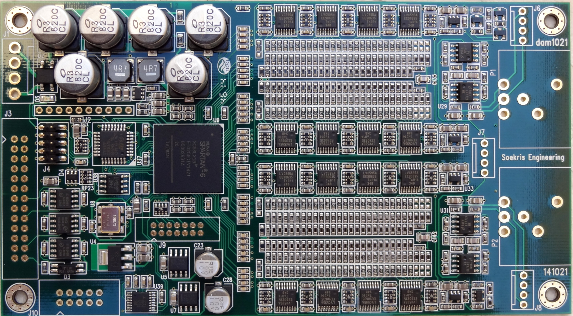
Note: in the diagram above the labels for “RIGHT CH” and “LEFT CH” are swapped. This was noted in the forums [1147] and I also checked it with a R/L test track.
The correct channel assignment (when viewed from the output side) is:
- Right Channel is on the right hand side
- Left Channel on the left hand side

NOTE: it could be possible to swap channels in software, but not possible with the current version of the firmware. Channel assignment is required for mono operation.
Update: firmware 0.99 [link] allows you to configure the DAC as MONO Left or MONO Right, but you still cannot swap the channels.
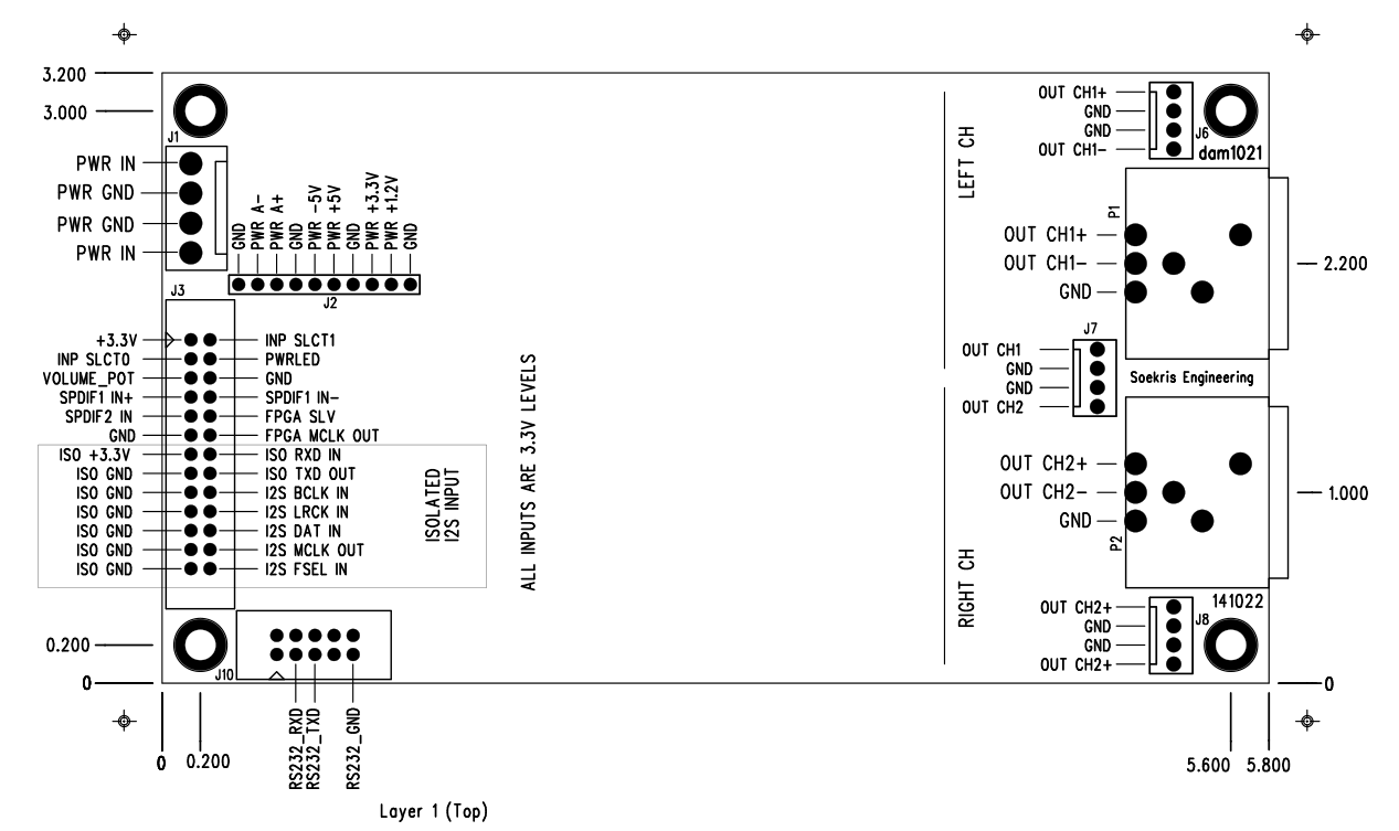
AUDIO INPUT CONNECTIONS
The dam 1021 supports the following input connections:
- Two SPDIF inputs.
- One Isolated I2S
SPDIF Inputs
You may use one for Toslink and one for transformer isolated Coax as follows [1108]
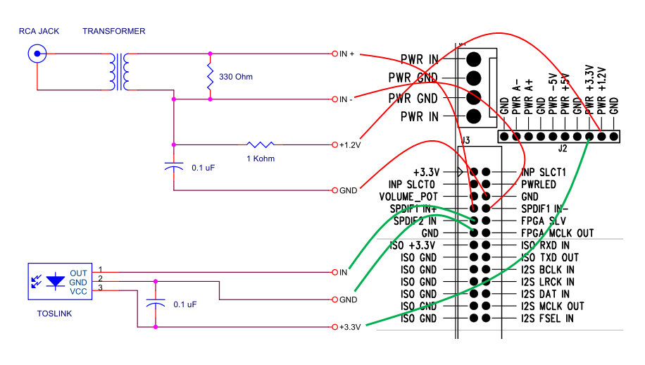
Notes:
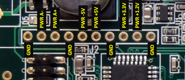
1.2v and 3.3v power can be taken off the DAC board as indicated in the diagram.
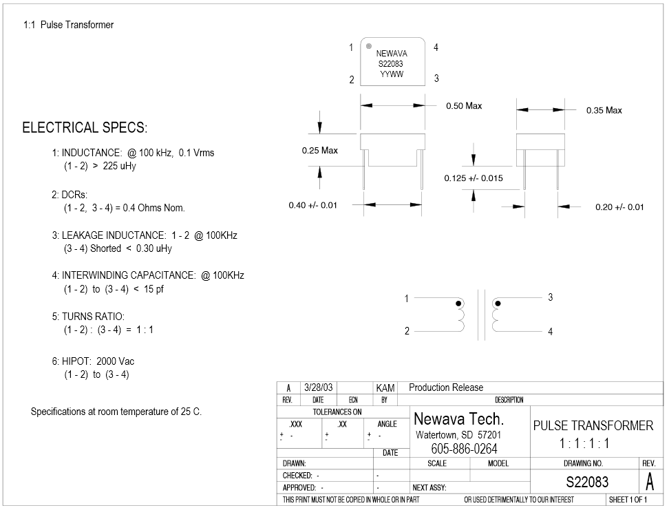
The isolation pulse transformer for the COAX input is a 1:1 type. The Newava Technology Inc S22083 is a favorite [link]. You may find more recommendations in the diyaudio implementation thread [link]
A toslink receiver can be wired as shown in the diagram. The Toshiba TORX147 [link] is a favorite. Seems Toslink receivers are hard to find in the component stores. eBay seems a good source [link]
A nice Toslink module is the one from Twisted Pear Audio [link]. (It is the one I own). This one has an on-board 3.3V regulator (IC1 in the diagram below) and is to be powered by 5-12V DC. This one has the Toshiba TORX142 module (25Mb) with supports up 192KHz sample rate (data sheet: torx142l), but Toshiba stopped making them. The current one that is on sale at the TwistedPear Audio store is specified to support up to 96KHz and uses the popular and current Toshiba TORX147.
DIYINHK Also has a very inexpensive ($4.00) Toslink receiver: [link]

The difference with the one from TPA is the lack of a local voltage regulator, so you need to provide 3.3V power (which is readily available from the DAC board)
I2S Input (Isolated)
The dam 1021 DAC implements a FIFO reclocker and therefore it does not need master clock input. It works similarly to many modern DACs where an internal PLL or equivalent circuitry locks to the bitclock and generates its own master clock.
The I2S input lines are also noise-isolated with Silicon Labs digital isolators [link]. This means that power needs to be provided to the isolator chips.
Thus the following connections are needed
- Connect I2S source BCLK to DAC I2S BCLK IN Pin
- Connect I2S source LRCK to DAC I2S LRCK IN Pin
- Connect I2S Data to DAC I2S DAT IN Pin
- Provide source 3.3V to ISO +3.3V Pin
- AND connect I2S GND to ISO GND
You may also also tap into a 3.3v line in the I2S source if an external supply is not available.
Here is an example using diyinhk USB to I2S adaptor:

The I2S wires (the multicolored ones)

5V for the ISOLATED INPUTS
According to the data sheet of the the Silicon Labs digital isolators on the board [link], the supply voltage can be 3.3V or 5V. With 5V you can use I2S inputs that are 5V. I have been using 5V supply and works well with 3.3V input signals.
Note that the isolator works by having separate power supplies on each side: the clean side (which is the DAC) and the “dirty” side (which is the I2S source). In order to provide complete digital isolation – meaning “isolated power and ground”, the two supplies must be completely separate. More here [link].
The power supply of the clean side is provided by the DAC board and cannot be externally accessed. The power supply for the “dirty” side is (and must be) provided externally.

Input Selection
The DAC supports automatic or manual input selection as follows:
| Input | INPSLCT0 Pin (J3) |
INPSLCT1 Pin (J3) |
Description |
| Auto Selection | Open | Open | DAC will search the 3 inputs for a valid signal and lock when a valid signal is found |
| I2S | GND | GND | Note that even when not used the USB-I2S interface might output a clock that the dam1021 lock on to…. |
| SPDIF 1 | Open | GND | This input is a sensitive LVDS Receiver -used for Coax [1076] |
| SPDIF 2 | GND | Open | This input is a standard 3.3V digital level -used for Toslink |
I recommend you try Auto Selection first (there is nothing to do). It works very well. Then if you have several sources and more than one active at any time, then implement some circuit (or use an Arduino) to select the desired input.
Signal LOCK indicator
- Steady on: signal lock
- Blinking: no signal or no lock

AUDIO OUTPUT CONNECTIONS
The dam1021 DAC provides the following outputs
- Stereo single-ended RAW outputs
- Stereo balanced buffered outputs which can also be used single-ended
- Both outputs are active and can be used concurrently
RAW outputs
The raw outputs come straight from the resistor ladder passing just through a low pass RC circuit. Raw outputs provide the cleanest, unprocessed output possible most desired by audio purists. It can be connected directly to an amplifier which typically have high input impedance (>10K ohm).
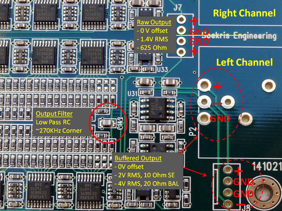
Note: Balanced offset has been measured to be 2V [link] -need to confirm…
Buffered Outputs
The raw output signal is also routed to a buffered single-ended to balanced signal converter as shown in the following diagram:

Buffered Outputs Balanced Connection

Buffered (and RAW) Outputs Single-ended Connection

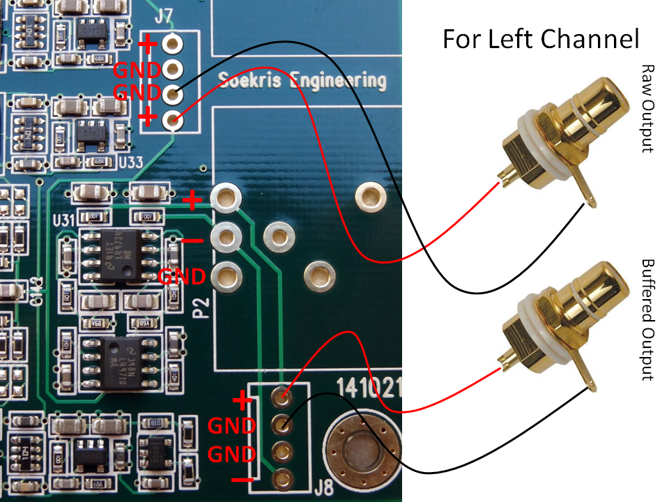
The buffered outputs are designed to drive high impedance headphones directly. Here is an example connection to headphone outputs:


I am using a Sennheiser HD-580, with a 300 ohm nominal impedance [link]. Sounds fantastic.
CAUTION: direct connection to an amplifier can result in passing the power on/off pops of the DAC potentially causing damage to the speakers. Follow proper power on/off management: turn the DAC on before turning on the amps and turn the DAC off first before turning off the the amps turn the amps off before turning the DAC off. This power sequence will ensure that the pops will not go through the amplifier circuit to the speakers.
If you are using direct connection (of the buffered output) to a headphone, the pops would be annoying but, at least in my case, they would not damage your headphones.
DIGITAL VOLUME CONTROL
Reference: [link]

The built-in digital volume is enabled with a potentiometer connected as such:
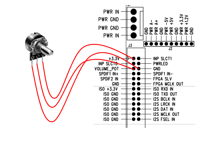
The nominal value for the pot is 10K ohm but any pot would probably work because it is used to set a voltage between 0 V and 3.3V to pin “VOLUME_POT”.
The typical configuration of a potentiometer is the one shown above where the middle pin is the wiper and the end pins are the end connections to the resistance. If you find that your potentiometer does not work as intended you can follow this simple method:
- Find the two “end” pins by measuring the resistance as you move the knob. When then resistance does not change when turning the knob, those are the “end” pins that connect to 3.3V and 0V. The third pin goes to the VOLUME_POT pin
- If you experience that volume decreases when turning the knob clockwise, reverse the connections
If nothing is connected, the volume level defaults to 0 db.
The advantage of using a potentiometer, as compared to using a rotary encoder (which at the moment is not supported anyway), the DAC always starts with the last volume setting.
POWER CONNECTION
The DAC implements several local regulators and therefore it is designed to operate out of a single center-tapped transformer. It can also work with DC input.
The requirements and specifications for the power supply or transformer are as follows [901], [848], [1130]
- DC: +/- 7.5V DC to +/-15V DC; preferable 9-12V DC
- AC: dual secondaries 2x 7-8V AC or center-tapped 0-16V AC
- Power consumption: 2.4V. Thus a 5W transformer is preferred
Transformer Hookup
A favorite transformer is the Hammond 229 series [link] it is a “dual-split bobbin” design with low EMF radiation. It is a step up from the standard low cost transformers.

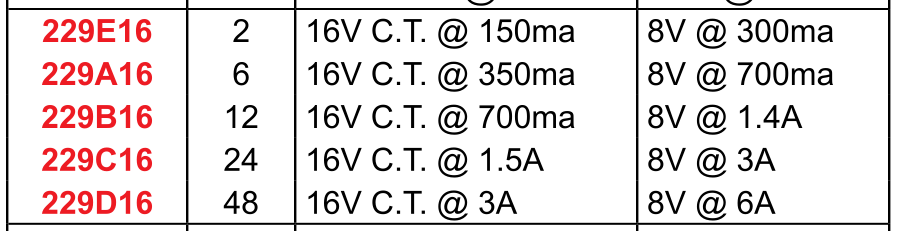
A 229B16 (rated at 12VA)would be an excellent fit with ample power for DAC. It is available at Digikey for about $16 [link]
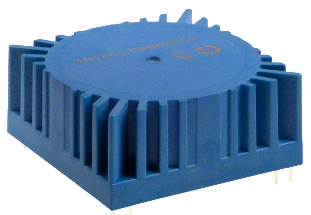
Another option is a low voltage toroidal transformer. A good example is the Amveco 70050 rated at 10VA [link]

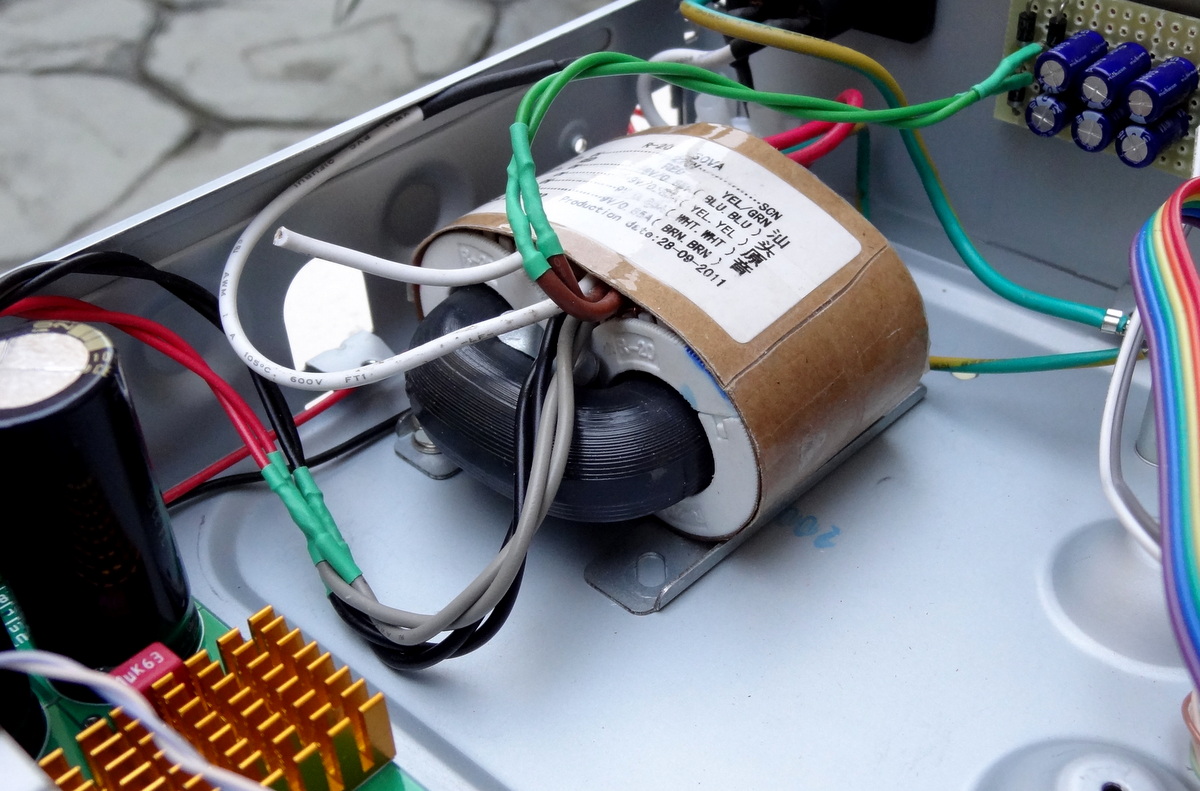
The basic hookup of a transformer to the DAC is as follows:

WARNING: AC MAINS voltage can cause death. If you don’t know what you are doing, don’t handle mains voltage.
DC Supply Hookup
The basic supply would be a bipolar +/- 12V supply. A low cost 78xx/79xx-based regulators would be good step up from a transformer-only supply
Note: the on-board bridge rectifier is a fast/soft switching bridge and a low cost DC supply comes with standard diodes/bridge – you may be trading off regulation with increased high frequency noise.
You can find plenty of adjustable supplies on eBay for very little money:
Or better yet, get a higher quality one from diyinhk which includes name-brand components:

The basic hookup is as follows. Notice that if you use a regulated supply, you need to increase the voltage of the transformer. A rule of thumb is to use the same AC voltage as the DC voltage.

Users have reported improvements from using a regulated supply over a transformer only supply [link]
…We started with the DAM as it was, with the Salas BiB (low noise regulated supply). We then unplugged the Salas and hooked up the plain transformer.
The change was immediately obvious. The sound thinned, it became more harsh in the high end. It also lost resolution and detail. Going back to the BiB made all the good qualities come back.
FIRST TIME POWER ON
Turn the power on and measure the voltages through J2 to ensure proper operation:
The analog power: PWR A- and PWR A+ depends on your input voltage. For a DC value of 12V you will see approximately 11V because of the voltage drop in the bridge rectifier.
SOFTWARE INTERFACE
Like many modern DACs, the dam1021 has a software interface. You can control the DAC with a micro-controller or a PC, update the firmware and upload custom digital filters.
In most DACs, the communication protocol with the DAC is I2C. In this DAC is serial communication. The dam1021 has two serial interfaces:
- Noise isolated TTL-level serial (not enabled as of this writing)
- RS232 serial (enabled with first release)
Communicating with RS232 Interface
Also check dimdim’s blog which has an excellent writeup on the RS232 interface [link]. Here I document my own experience with the interface.
You need:
- PC serial port
- Or a USB to RS232 interface cable capable of supporting 115,200 baud
- Note: The serial port transceiver on the dam1021 R-2R DAC has power savings enabled, to reduce noise. It needs valid RS-232 level on the RXD line to power up. If your USB-Serial dongle also have power saving then you have a problem. [1176]
- Terminal program
Hardware connection
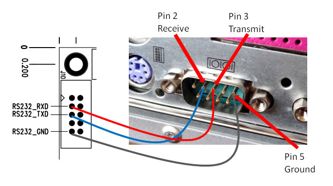
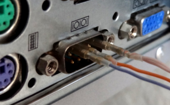
Connect the RS232 pins to the PC serial port as follows. This is basically a null-modem connection without h/w flow control. You may want to check this informative site on serial communications including RS232 [link]
I made a simple 4-feet cable with 2 twisted pairs of cat-5 wires.
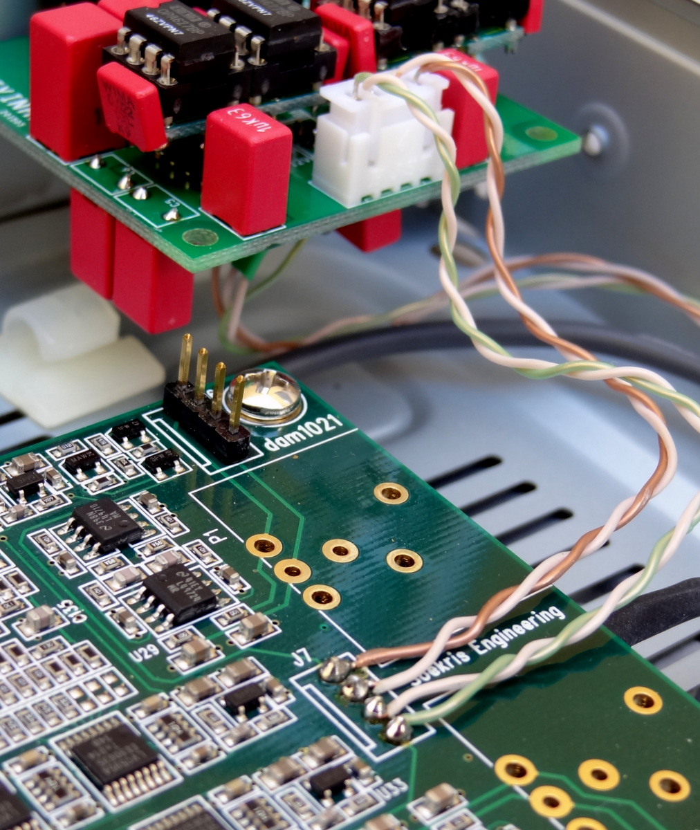
Notice the pins in the board can also be numbered 1-5 counting from the top right in the photo. So pin 2 in the PC serial port goes to pin 3 in the DAC, pin 3 to pin 2 and pin 5 to pin 5.

One can interface with the DAC in two modes:
- Interactive by invoking the “uManager” and using a terminal application
- Non-interactive by sending messages to the DAC through the serial port (with or without a terminal application)
Using Terminal Application (Tera Term)
The terminal program must support xmodem file transfer protocol. Putty is a very popular terminal program but does not support xmodem. “ExtraPutty” is an offshoot of Putty and supports xmodem, but it requires .NET but I didn’t want to download .NET. I ended up selecting “Tera Term”. Check the use of ExtraPutty in dimdim’s post [link]
Download Tera Term from [link]
After downloading and extracting all the files, launch the application “ttermpro”

After launching Tera Term, select “Serial” and select the Port you are using to communicate with the DAC.
Configure the serial communication parameters with:
- Baud rate: 115,200 (This is pretty fast. Use a good, short cable)
- Data bits: 8
- Stop bits: 1
- Parity: none
- Flow control: none
Click on the “Setup” pull-down menu and select “Serial port”
Invoking “uManager” for Interactive Mode
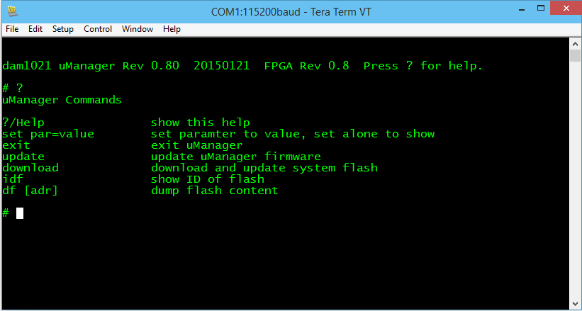
Type “+++” and wait for the DAC to respond (~1 sec). You must enter “+++”, otherwise there will be no response. If you enter anything else, there will also be no response. “+++” invokes the “uManager” enabling interactive communication with the DAC through a terminal window. The DAC also responds to commands sent through the serial interface (more of that later)
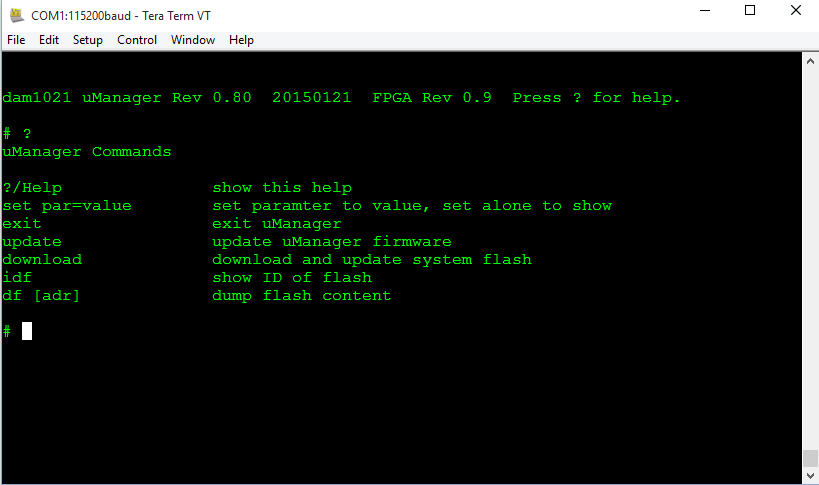
The dam1021 will respond with the following screen. Notice the original firmware is “FPGA Rev 0.8”

Typing “?” returns a list of available commands
Updating the firmware
First download the firmware from [1116] and unzip it (it is a “SKR” file):

Type “download” in the terminal window. The DAC will acknowledge your command and wait for you to start the xmodem transfer.
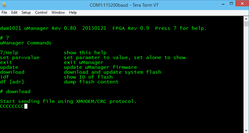
In the “File” pull down menu select “Transfer” -> “Xmodem” -> “Send” and you will see the XMODEM send dialog box. Select the file you downloaded and click “Open”

The file will start transferring and you can see progress in the progress bar.

After completion, [optional – type “exit” in the terminal window] power cycle the DAC. Type “+++” in the terminal window and wait (~1 sec). You will see the following screen. Notice that the firmware version is now 0.9

Non Interactive Commands
You may send commands to the DAC through the terminal application but without invoking the “uManager”. If you are in uManager, type “exit” to exit uManager. The DAC is then ready to receive messages/commands.
UPLOADING DIGITAL FILTERS
Now that we know how to update the firmware, uploading digital filters uses the same procedure. Lots of filters have been crafted by users in the diyaudio filter brewing thread [link]. Filter files ready to be uploaded are binary files. The filter text files cannot be uploaded. They need to be converted to binary format with the “filter tools” provided by Soren [link]
The procedure for uploading a filter file is hereby summarized:
- After invoking the uManager, type “download” in the terminal window. The DAC will acknowledge your command and wait for you to start the xmodem transfer
- In the “File” pull down menu select “Transfer” -> “Xmodem” -> “Send”. You will see the XMODEM send dialog box. Select the filter file you wish to upload and click “Open”
- After completion, power-cycle the DAC. Note: changing the input or changing a track with a different sample rate also triggers reloading of the filters
MASTER CLOCK OUTPUT
Ref: [848]
- I2S MCLK OUT pin: Master clock output: 45.1584 and 49.152 Mhz (which can also be divided)
- I2S FSEL IN pin: Input signal at this pin selects between 45.1584 MHz and 49.152 MHz master clock output
Although not advertised as working with the initial firmware, it has been reported to be fully working as indicated above. [link]
MY OTHER POSTS ON THIS DAC
| TITLE | SUBJECT |
LINK |
DESCRIPTION |
| Soekris dam 1021 R-2R DAC ILLUSTRATED GUIDE | Users Manual | [link] | Users manual for the Soekris DAC. |
| Soekris dam1021 Build | Build Guide | [link] | Details of my initial build of the Soekris DAC. |
| dam1021 R-2R DAC MODs | Mods | [link] | Mods I have performed on the DAC build. |
| dam1021 R2R More Mods | Mods | [link] | Later mods on the DAC build. |
| Digital Filters for Soekris R2R DAC | Digital Filters | [link] | Extensive list of DIY filters from the diyaudio filter brewing forum thread. |
| R2R Benchmark Filters (for now) | Digital Filters | [link] | Latest set of filters developed and shared in the diyaudio filter brewing forum thread. The best filters of the bunch. |
| R-2R DAC For The REST of US | Technical Details | [link] | Introductory post describing the innovations and capabilities implemented in this DAC. |
| The Soekris R-2R DAC: Technical Details | Technical Details | [link] | Additional technical details of the Soekris DAC that were not covered in the post above and collected after I had the DAC on my hands. |
dam1021 R-2R DAC MODs
BEST FREE MOD: Board Isolation
Eliminate ground loop
To eliminate the ground loop I was experiencing with the external RCA connectors I had to isolate the RCA connectors from the chassis. That did not explain the source of the ground loop though, it merely eliminate the additional path to signal ground. I had no supply ground wires connected to chassis and the only ground connection to chassis was the safety EARTH ground, so where did the ground loop come from?
After some poking with a voltmeter, I figured the real source of the ground loop. The mounting holes of the DAC board are encircled with ground pads. These short to the mounting posts and the mounting posts short to the chassis.
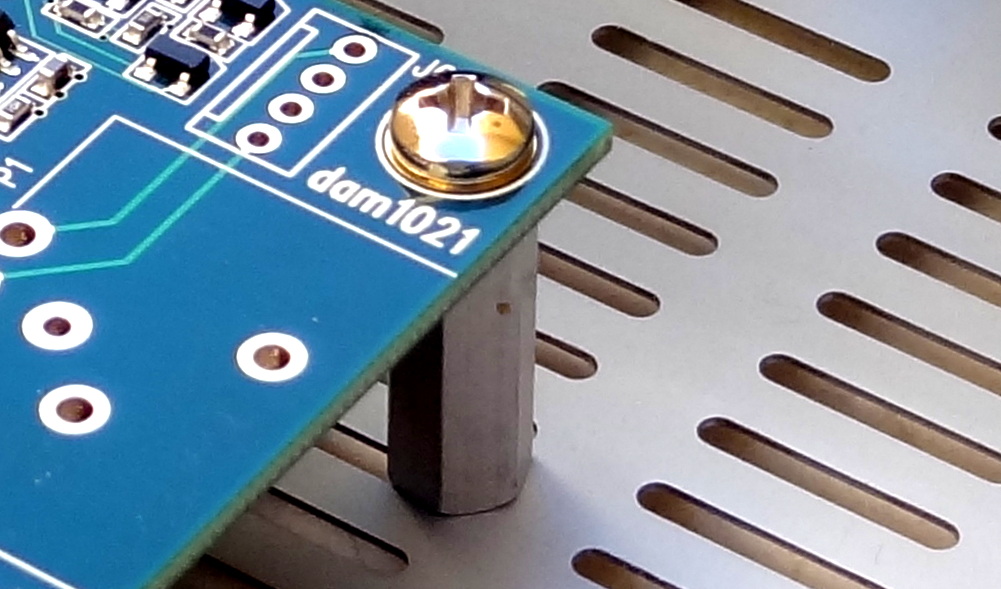
If you don’t have an alternative path (for the signal) to ground, then you don’t have a ground loop. Having signal ground connected to the chassis is probably a safety feature but for audio, it is best to avoid it. I have built all my electronics with the signal ground (the supply ground) isolated from the chassis and to ensure safety I use a 3-wire power cord with the EARTH ground wire (the green wire) connected to the chassis.
If you don’t have the chassis connected to ground, then having the signal ground connected to the chassis could create a dangerous situation in the even of a short, energizing the chassis.
If using the chassis to shield sensitive electronics, then it is certainly a good idea to not share the chassis ground with the electronics/signal ground.
So I think it is always a good idea isolating the board from the chassis (and using earth ground to ground the chassis)
Isolation washers
To isolate the mounting posts, I made poly washers for the mounting screws and put them on the top side and bottom side of the board:

These were made from presentation transparencies (remember those?) with a regular 3-hole paper punch and then using a smaller craft punch for the center hole. The came out very nice.

Improved SNR
Mr. dimdim measured the noise improvements after isolating the board [link]:
… The installation of the α20s had coincided with me changing my plastic IEC with a metal one, that also provided filtering. Metal (IEC) meant that the main’s GND would be connected to my chassis. You may remember that the Soekris does not have insulation on its mounting holes, so if you are using metal standoffs to mount it you are effectively connecting your signal ground to your chassis.
To make a long story short, isolating the DAM from the chassis improved the noise floor by a whopping ~23dBs. It also made significant difference in the dynamic range, THD, etc.
There you have it! The best free mod.
INITIAL POWER MODS
The power on/off POP seems benign if listening through headphones. The power ON pop is not loud at all but the power OFF pop is loud. If connected directly to an amplifier, it can potentially damage the loud speakers (I have not tried it, so far listening with headphones).
During Power off, the positive rail drops faster than the negative rail and this creates a voltage imbalance resulting in a huge POP. At some point, the device is practically powered by the negative rail [link]. The effect can also be visually seen:
The left LED is on the positive supply. It goes dim first when cutting the external power.

I attempted to balance the power consumption for the two rails hoping to reduce the turn-off POP.
Adding capacitors to the positive rail
By trial and error, incrementally adding capacitors up to 13,000 uF I was able to balance the power decay between the positive rail and the negative rail by visually matching the turn-off rate of the two LEDs in the supply. The POP was somewhat reduced (using headphones) but not eliminated.
Adding resistors to the negative rail
I then tried to match the current consumption of the negative rail with the positive rail. The power consumption of the DAC is: [1130]
- Positive Rail: .18A, 10V
- Negative Rail: 0.06A, 10V
I added enough resistors to increase current consumption by 120 mA. I used 10 1 Kohm resistors on the -12V leg of the supply. Each would dissipate 12 mA of current and .144 W of power -they are rated at .25 W, so we are safe.
The result was better than adding capacitors to the positive rail, the POP at power off was further reduced but still not eliminated. I liked this mod better than adding capacitor, so I made it permanent in the supply.

Note: only tried with headphones. And yes it is a waste of energy, but it is only 1.4W 🙂
BYPASS THE BRIDGE?
An apology to my readers for putting up wrong information.
I took a closer look at the J2 connections on the backside and the board and the +/- analog power connections are connected to the power lines after the RC filter. If you power through J2, there will be a 12 ohm resistor to the filter/smoothing caps. This would not destroy the board, but it is not the right design/thing-to-do either. Thus there is no good reason to power through J2.

The white arrows point at the +/- analog power traces:

ADDING CAPACITORS
While examining the back of the board and realizing that J2 cannot be used as input power, I figure it is the perfect place to add capacitors to the power supply lines. Decided to add 330 uF Oscons to the digital 1.2V and 3.3V and Panasonic FMs to the +/- analog lines. This mod is completely reversible. Just cut the leads. I first soldered a row of pins and the capacitors are soldered to the pins as shown in the photo below.
Adding capacitors to the analog lines further improves the filtering because it adds capacitance to the RC filter.
There is still the +/- 5V lines but there is no more space. I also chose not to add capacitors to these lines because the 5V regulators already have large output capacitors, and because I thought they would benefit the least: if you examine the backside of the board, you’ll notice that the connectors at J2 trace back from different places in the board. The longest traces are from the +/- 5V regulators.

The capacitor added to the 3.3v supply connects to the 3.3v power plane through a short trace (the straight vertical trace under the pins of the left capacitor).

These power mods are “approved”: [link]
If you insist to improve the on-board power supply, try replacing the 6 electrolytic capacitors with aluminum polymer types, 1000u 16V exist in same 10mm SMD footprint and t.ex. digikey stock them at $2.20 each. Should be easy to replace.
You can also add a small polymer electrolytic on the 3.3V output, but please note that the clock oscillator power already have a filter, so I doubt it will make any difference.
Didn’t want to remove the existing capacitors and risk damaging something. It is too early to do any kind of surgery on the board :-). Plus the existing filter capacitors don’t seem quite easy to remove given that there is very little space between them.
FULL DIGITAL INPUT ISOLATION
These are the Silicon Labs digital isolators on the board [link]. I believe the original ones in the engineering board were TI isolators [link]. Both isolators use the same capacitive coupling technology. I suspect the Si parts have equivalent performance when it comes to noise isolation.
According to the diagram below, the parts can also be used for logic level translation and thus they can be powered with 5V on the input. This will make the input compatible and tolerant to 5V signals such as those present in a serial interface of a standard Arduino microcontroler.
5V tolerance is also needed if interfacing to the I2S/serial signals of older generation CD players when they used spend good engineering money in making CD-only players. I like older CD-only players as compared to modern multi-format players because they are better made, start up/play much faster and the drawer mechanism is also much faster. You don’t have to wait for the device to check the format, read the contents, etc before it starts playing. If you click “eject”, it immediately ejects; no need to wait for the device to do who knows what before it ejects the disc.

To reduce overall system power consumption, many of today’s high-speed logic devices (e.g. FPGAs) operate from supplies of 3V or less. Lower bias voltages (and consequently lower logic thresholds) complicate interface with 5 V devices, creating a need for a fast and robust logic level shifter… the Si86xx isolator (can be) used as a logic threshold level shifter where each side of the isolator is biased to match the local logic rails. Note the common ground on both sides of the isolator since alllogic supplies are assumed to be connected to a common ground.
However, I don’t have to assume that the logic supplies are connected to a common ground and instead I am going to isolate the two grounds as much as possible by powering the input side with a completely separate supply, including using a separate AC transformer.
I salvaged another transformer (this one gives 9V DC unloaded) and a 7805 series LDO regulator

I had to rearrange the supplies in order to fit them in the chassis. This arrangement is even better as the line voltage components and wires are confined to the left-most area of the case and as far as possible from the low voltage electronics.
MY OTHER POSTS ON THIS DAC
| TITLE | SUBJECT |
LINK |
DESCRIPTION |
| Soekris dam 1021 R-2R DAC ILLUSTRATED GUIDE | Users Manual | [link] | Users manual for the Soekris DAC. |
| Soekris dam1021 Build | Build Guide | [link] | Details of my initial build of the Soekris DAC. |
| dam1021 R-2R DAC MODs | Mods | [link] | Mods I have performed on the DAC build. |
| dam1021 R2R More Mods | Mods | [link] | Later mods on the DAC build. |
| Digital Filters for Soekris R2R DAC | Digital Filters | [link] | Extensive list of DIY filters from the diyaudio filter brewing forum thread. |
| R2R Benchmark Filters (for now) | Digital Filters | [link] | Latest set of filters developed and shared in the diyaudio filter brewing forum thread. The best filters of the bunch. |
| R-2R DAC For The REST of US | Technical Details | [link] | Introductory post describing the innovations and capabilities implemented in this DAC. |
| The Soekris R-2R DAC: Technical Details | Technical Details | [link] | Additional technical details of the Soekris DAC that were not covered in the post above and collected after I had the DAC on my hands. |
Soekris dam1021 Build
Please also refer to:
Here is my board (S/N 000003) and even personally signed by Soren :-). I will document my build in this post.
POWER SUPPLY
Just finished building a +/- 12V power supply and had it powered-on an entire day in order to ensure that nothing was wrong with it. Most of the components are from my “pile of electronics”: some now, some recycled.
The transformers were taken from “surplus” unregulated wall supplies and are rated at 15V AC (which are too high of a voltage to use directly on the DAC board).
It is as basic and standard as a linear supply could be.

The AC rectifying part is basically the dam1021 input section
- Two transformers (AC 15V)
- Single bridge (2A)
- Smoothing capacitors. In this case 35V, 2200 uF standard Nichicons, one per rail
The regulators are fixed output voltage LM7812 [link] and LM7912.[link]. Could have used adjusttable, but did not have a negative LM337 at hand.

The film caps are additional bypass close to the regulators.
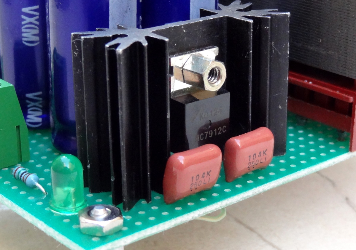
The “hardest” part of the build was manually placing the components on the board for a good fit. Maybe a CAD layout tool would had been a great help.

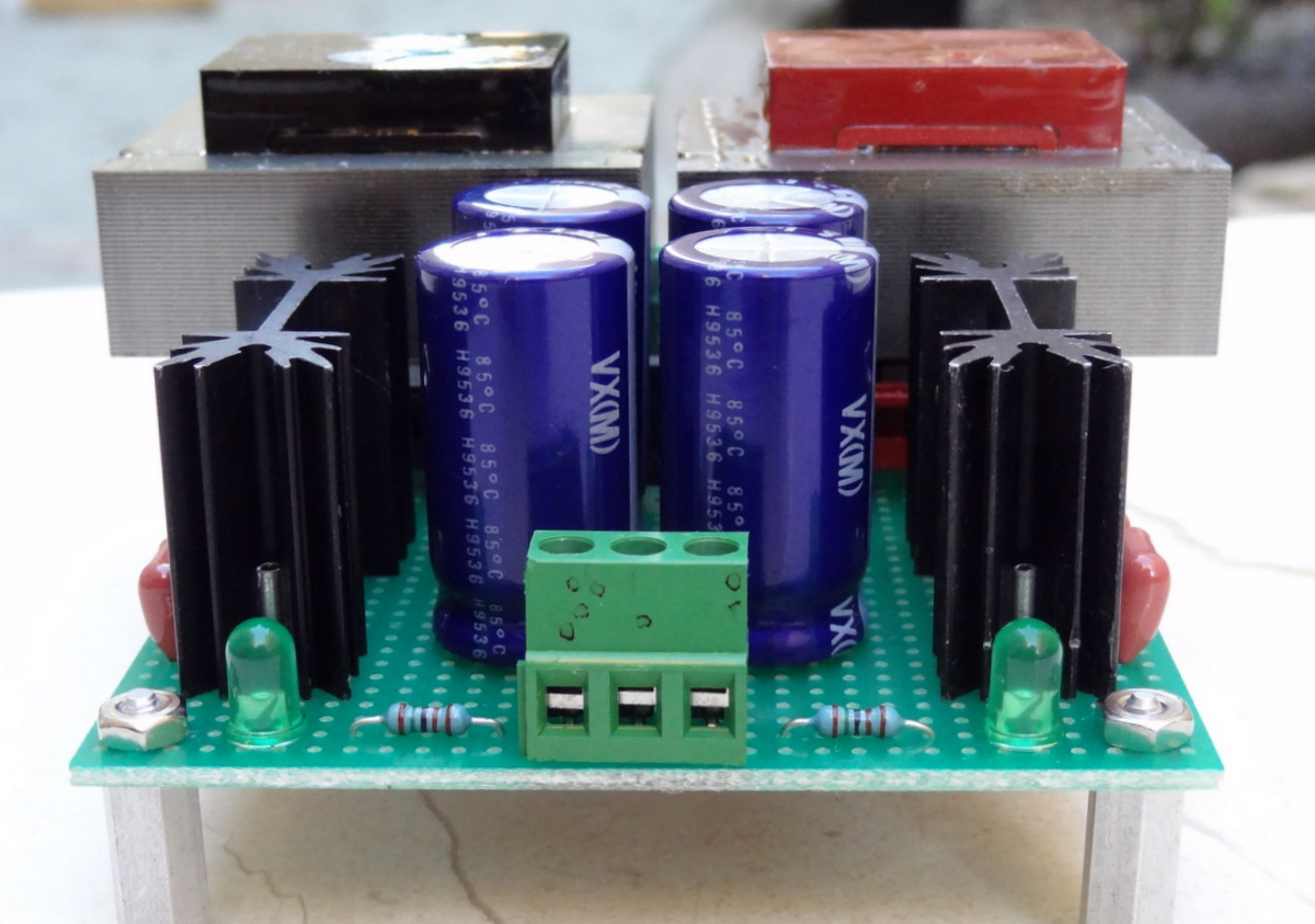
Not very pretty, but works fine. The thicker wire in the center is GND.
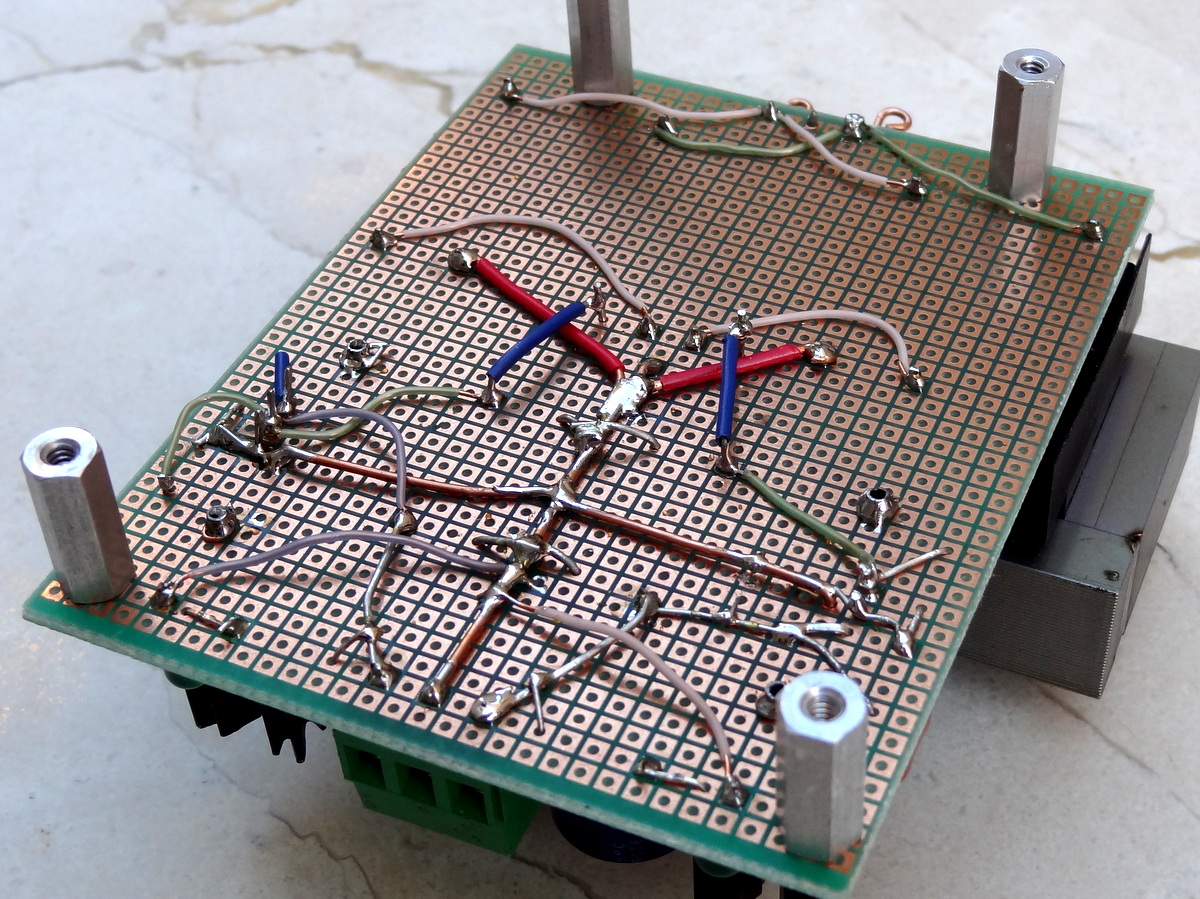
If building the PS from scratch is too much of a hassle, there are many kits from eBay for very little money. (You still need to source the transformers). The most popular ones are the adjustable ones based on the LM317/LM337. One good example is the following kit [link].
POWER SUPPLY MODS
For now, I am not thinking about PS mods, but here is a post with a lot of good information and measurement on the DAC in general and particularly on the power section [link].
After reading the post, these are some of the things that come to mind:
Reducing Power On/Off POP
During Power off, the positive rail drops faster than the negative rail (remember that the positive power consumption is 3X negative power consumption) and this creates a huge POP when the device is practically powered by the negative rail. – Using the additional capacitance of the regulated supply would probably make this problem worse because the capacitors are equal in size between the positive rail and negative rail.
The left LED is on the positive supply. It goes off first when cutting the external power
Possible solutions:
- Increase the power draw of the negative supply to be equal of the positive supply: you can do this by adding resistors to ground on the output of the supply.
- Adjust the amount of capacitance between the two rails so that during power off, the voltages on the two rails decay in approximately equal rate. This may or may not work, but it sounds that it could.
- Separate the analog supply (opamp and voltage reference) from the digital supply which only uses the positive rail. This requires major surgery of the board.
Snubbers on the transformer
The shouty sound can be somewhat tamed by filtering the power line and using optimal snubbers for the power transformer. (Check the Quasimodo/Cheapomodo threads for an excellent snubber measurement jig by Mark Johnson.)
Bypass bridge rectifier (this also “skips” the smoothing capacitors)
Update: I took a closer look at the J2 connections on the backside and the board and the +/- analog power connections are connected to the power lines after the RC filter. If you power through J2, there will be a 12 ohm resistor to the smoothing caps. This would not destroy the board, but not the right design. (It is actually safe [link]). This is probably only useful if you have a well filtered and regulated DC supply and you are operating near the headroom required by the 5V regulator which is around 7V. In any case, it is better to power through J1.
If using a regulated supply for input power, it is possible bypass the built-in bridge rectifier which is used for AC input. For DC input it is basically serves no function except it adds extra protection in case you inadvertently apply the wrong polarity.
I measured the PWR A+ and PWR A- connections in J2 against the + and – poles of the input filter caps and I measure continuity.
It would be better to use the GND connections of the power input (the ones in J1)) since they provide a solid and hefty connection to the GND plane. The ground connections on J2 are through thin traces.

But I need to respect the manufacturer’s warning, so here it goes [link]:
I Repeat:
I can only recommend to supply any power on J1, the diode bridge used on the input is a low noise schottky type.
J2 is NOT for supplying power, it’s for testing or for sourcing small amount of power for external input circuits. Applying power will probably blow the board.
But on the other hand, just go ahead, I’ll be happy to sell you a couple of new boards 🙂
Connecting the input power this way, bypasses the bridge rectifier (and skips the smoothing capacitors. I say “skip” because it does not bypass them since they are still connected through a 220 ohm resistor).
Replacing and adding on-board PS capacitor
This one is endorsed by Soren [link]
If you insist to improve the on-board power supply, try replacing the 6 electrolytic capacitors with aluminum polymer types, 1000u 16V exist in same 10mm SMD footprint and t.ex. digikey stock them at $2.20 each. Should be easy to replace.
You can also add a small polymer electrolytic on the 3.3V output, but please note that the clock oscillator power already have a filter, so I doubt it will make any difference.
Here is the 3.3V regulator. You may add a capacitor between Vout and GND (pins 1 adn 2)

At this time I would be doing a standard installation before thinking of any other mod.
CASE
Old electronics are excellent for these projects. Not only they are free, but at the minimum you get athe power cord/socket installed and some even come with power filters.

This one has a power socket for a detachable power cord and ground safety (the green wire)

Lots of useless buttons, but not bad looking at all 🙂
Reusing the RCA connectors: one set for single-ended raw output and one set of single-ended buffered output
Perfect fit.

I like to use the analog-audio cable assemblies found inside (older) PCs. They have three leads (for left, right and ground) and are shielded.

OTHER COMPONENTS
Volume Potentiometer
It is recommended to use a 10K pot. (although a different value one might work as I beleive it is measuring voltage)
I am using one from a gutted Sony analog surround processor (when Japan used to make stuff :-)) which happens to be 10K potentiometer.

Toslink Module
I will be using what I think is the best Toslink Module: the original one from TwistedPear Audio. This one has the Toshiba TORX142 module (25Mb) with supports up 192KHz sample rate (data sheet: torx142l), but Toshiba stopped making them. I purchased this several years back with the OPUS DAC [link] (which got me started in this audio DIY thing). The current one that is on sale at the TwistedPear Audio store is specified to support up to 96KHz [link].
The module has an integrated 3.3V regulator [link] and thus it is compatible with the 3.3V input limit of the R-2R DAC. In addition, the regulator is specified to accept 5-12V DC (with a spec max of 18V). It can therefore be powered directly by the 12V supply. No need to pull the power from the DAC.
The case even has a cut-out for the Toslink module…
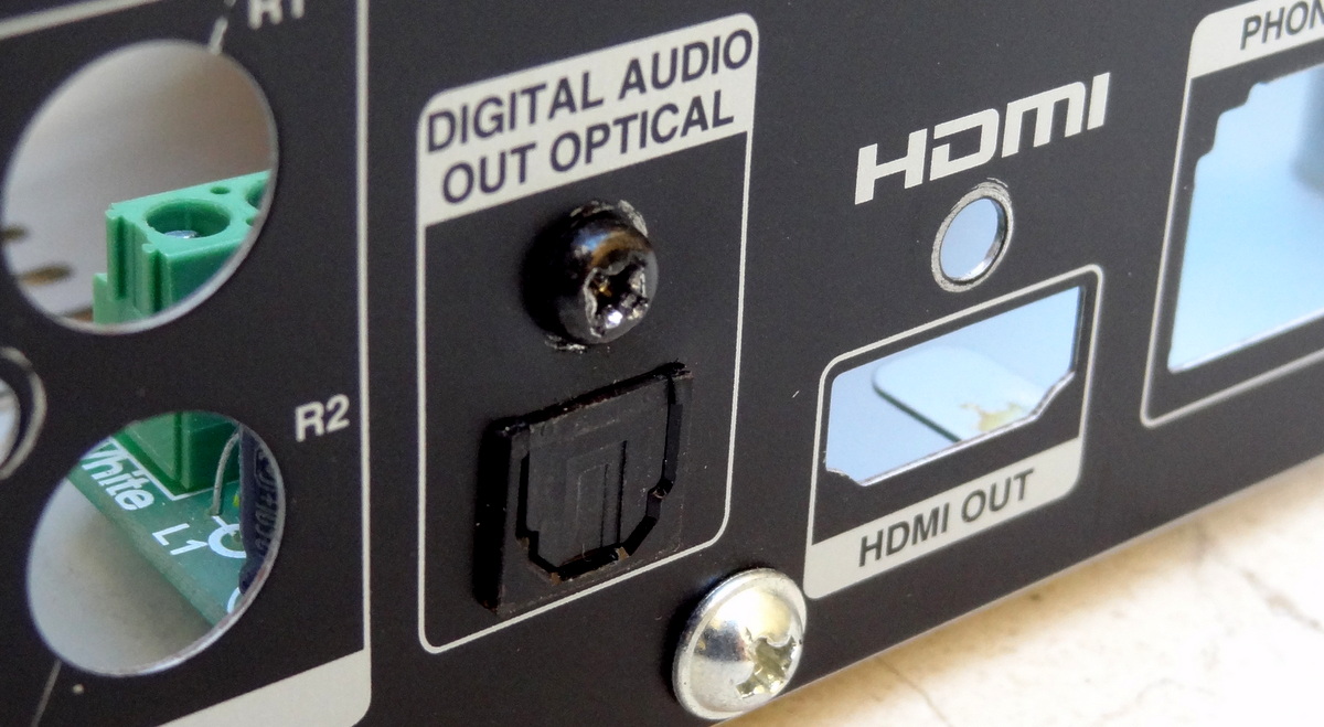
USB to I2S Module
I am going to use the original DIYINHK XMOS-based module [link]. This one is USB powered.
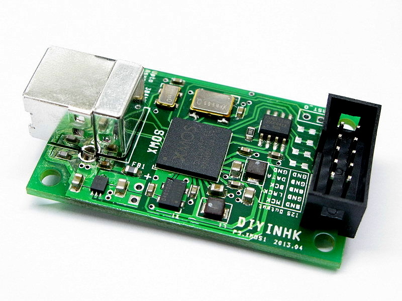
ALL TOGETHER
Wanted to first check out the DAC with a basic and default configuration: Toslink Input, volume control, and SE buffered output to headphones.
Power connections, volume control connections and SPDIF connection.
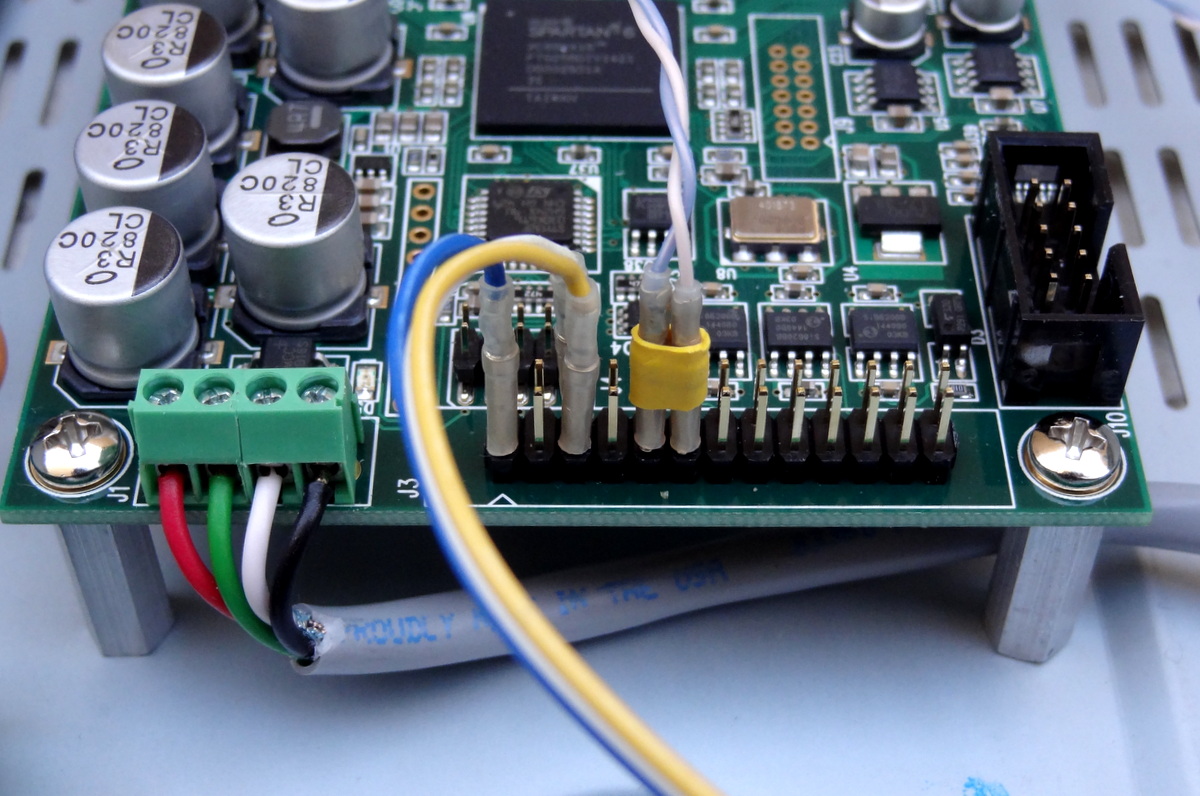
Single-ended buffered output to a front-panel headphone jack.
The output opamp, the LME49724 [link] can drive a high impedance headphone directly. It is specified to drive a 600 ohm load meeting full specification.
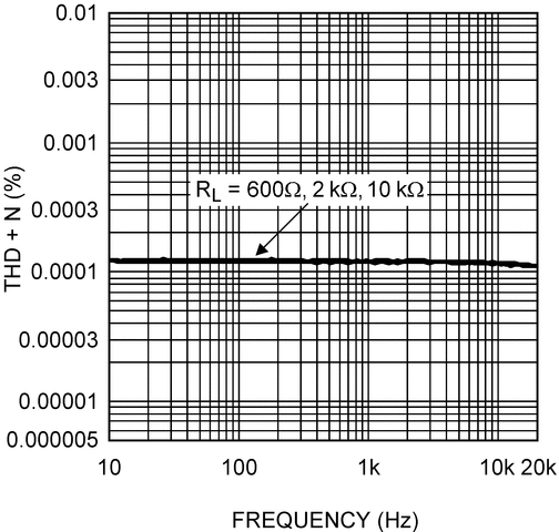
Since the Senn HD-580 I use has an impedance of 300 ohm, I expect only a slight deviation from the specification, if any.
Front panel: power LED (in the power button), toggle power switch, headphone jack and volume control
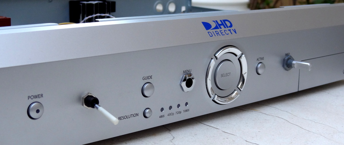
I also installed an RCA jack for coax SDPIF. The Toslink module is powered by the +12V supply. The USB-I2S is powered by USB.
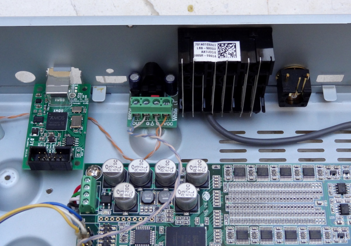
Back panel: SPDIF Coax, SE Raw output, SPDIF Toslink and USB-I2S
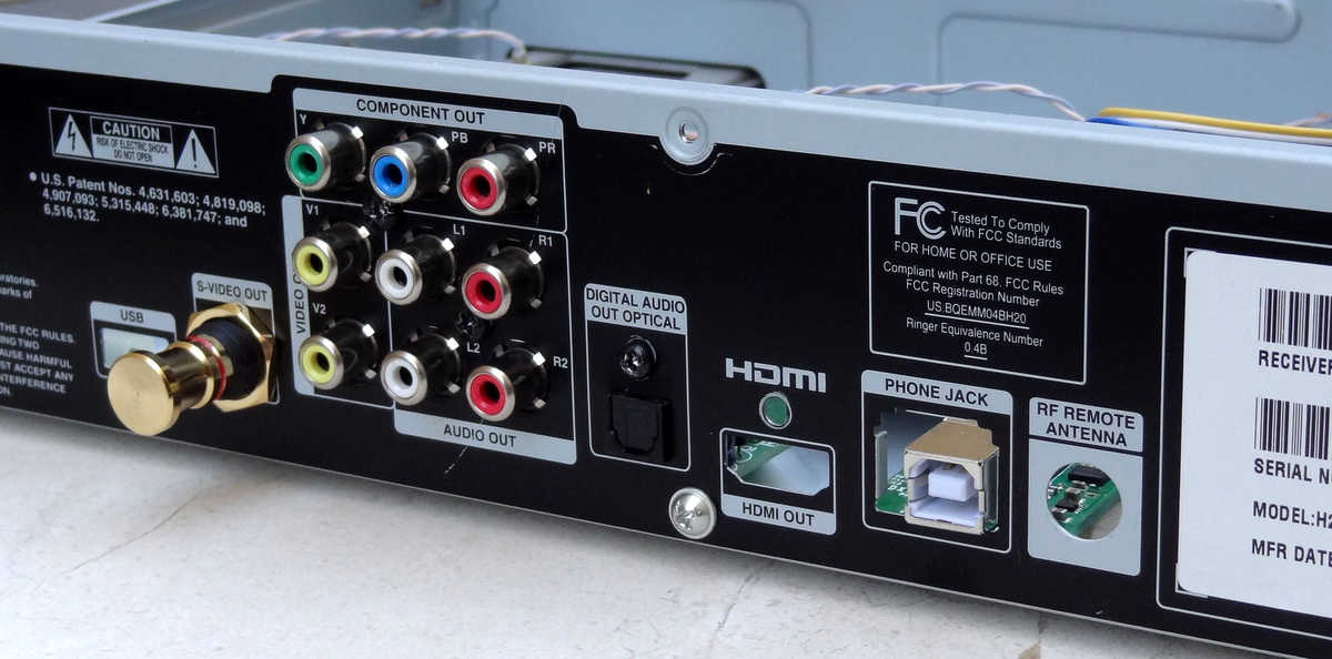

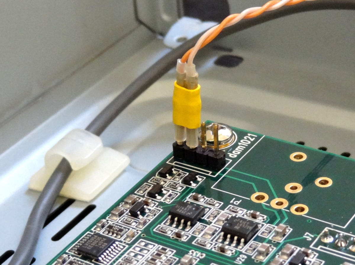
Just powered it up, original filters. Denon Multiformat player, Toslink output. Senn HD-580 (300 ohm) and Fidelio X1 (30 ohm).
INITIAL POWER-ON
No sound
First there was no sound either from the raw outputs or the SE buffered outputs.
- The signal lock LED was steady. In auto-input mode, the signal locks quite fast, as it should
- The voltages on J2 were all correct
- Removed the volume potentiometer connections, leaving just the SPDIF input
- Double checked all the output connections
It turned out that I had soldered the wrong connectors on the RCA jacks and the Headphone jacks!
Signal lock LED
- Steady on: signal lock
- Blinking: no signal or no lock
Hum
Then there was a hum coming from the raw output connected to the RCA jacks (RCA-Head Amp-Headphones). I figure there got to be a ground loop. I measured continuity between the chassis and the RCA GND.
Had to remove the metal plate that was grounding the outer sleeve of the RCA jacks to the chassis (the little metal tabs on each RCA jack).
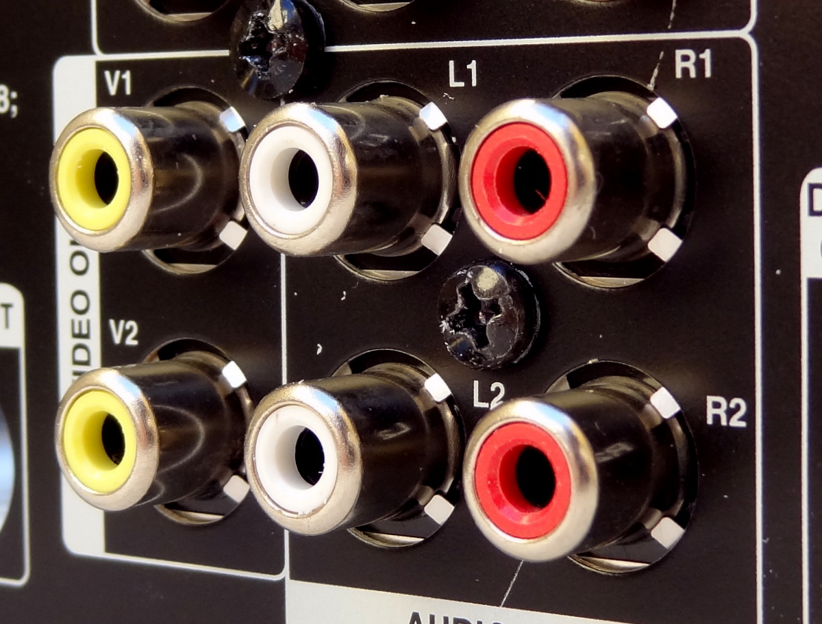
Volume control rustling/crackling noise
I hear a faint static-like click when adjusting the volume. It is like the old analog amps when the pot was dirty or worn out. But this is digital. I shall investigate this further…
I added a 0.1 uF capacitor between 3.3V and Gnd and between the wiper and Gnd. No improvement. I think the problem could be in software (the FPGA volume software)

HOW DOES IT SOUND
Using Toslink source from Denon multiformat player, single-ended buffered output to a Senn HD-580 headphone. Compared with the analog output of the same player through a Fiio top of the line headphone amp.
The immediate most noticeable thing in an A/B comparison with the Denon player is the larger soundstage of the R-2R DAC. Further listening indeed shows a more expansive soundstage, like each instrument and voice fills more of the space around it.
The bass is also more “full bodied” and more impactful. Beautiful bass. I am using the original filter and do not detect any “harshness” as others have.
Perhaps comparing with the Denon is not such a good comparison, but it was easy and shows the that DAC performs very well.
I shall try other filters. Perhaps then I would feel the original filter results in some harshness…
Also, with direct output, I prefer the HD-580 to the Fidelio X1.
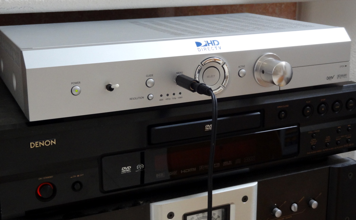
GOT THE I2S GOING
Finally connected the DIYINHK XMOS I2S module (this is the original model, different from what Soren is using -I believe the current isolated one).
Listening with iTunes and having iTunes upsample everything to 176.4KHz. Sounds good…
The DAC automatically selects the active input right away. On the XMOS device, once you apply power, there is bitclock and the DAC locks to it.
I am still using original firmware, so the slight clicks when changing sample rate are there. The rustling/crackling sound of adjusting the volume is also still there. I am sure these will be fixed, it the meantime, they don’t bother the listening experience.

In order to power the input side of the isolator, I had to build a small supply with a 5V regulator and a 3.3V regulator (didn’t have anything else suitable). The 3.3V regulator is a surface mount device so I had to solder legs and small heatsink tab. Just a crude but effective job 🙂

How does it sound?
Whereas in the previous comparison, the DAC showed a more expansive soundstage, and the bass was more “full bodied”, more impactful, using I2S input (Windows 7 laptop, iTunes 12 with upsampling to 176.4KHz 192KHz [Check my post on adjusting the iTunes playback sample rate [link] and diyinhk XMOS interface) results in another step forward towards better sound and a enjoyable experience. This time the improvement is presented as music with more clarity or “crispiness” (more details?) as though the instruments give out a more “defined” sound. I think this reviewer gives a pretty good description of what I want to say: [link].
MY OTHER POSTS ON THIS DAC
| TITLE | SUBJECT |
LINK |
DESCRIPTION |
| Soekris dam 1021 R-2R DAC ILLUSTRATED GUIDE | Users Manual | [link] | Users manual for the Soekris DAC. |
| Soekris dam1021 Build | Build Guide | [link] | Details of my initial build of the Soekris DAC. |
| dam1021 R-2R DAC MODs | Mods | [link] | Mods I have performed on the DAC build. |
| dam1021 R2R More Mods | Mods | [link] | Later mods on the DAC build. |
| Digital Filters for Soekris R2R DAC | Digital Filters | [link] | Extensive list of DIY filters from the diyaudio filter brewing forum thread. |
| R2R Benchmark Filters (for now) | Digital Filters | [link] | Latest set of filters developed and shared in the diyaudio filter brewing forum thread. The best filters of the bunch. |
| R-2R DAC For The REST of US | Technical Details | [link] | Introductory post describing the innovations and capabilities implemented in this DAC. |
| The Soekris R-2R DAC: Technical Details | Technical Details | [link] | Additional technical details of the Soekris DAC that were not covered in the post above and collected after I had the DAC on my hands. |
The Soekris R-2R DAC: Technical Details


The Soekris R2R DAC is finally out, officially named
The Soekris dam1021 Sign Magnitude R-2R DAC
I will be collecting useful information here and in other posts because as the thread at diyaudio gets longer, it would be difficult to find things…
USERS GUIDE: [link]
INITIAL FEATURES
The initial release (“v1) of the firmware together enables the following features:
- I2S input up to 384KHz sample rate (tested to 192KHz)
- SPDIF input up to 192KHz (tested to 96KHz)
- Automatic De-emphasis for 44.1KHz material
- Built-in set of simple FIR filters for all sample rates
- Digital volume control through simple potentiometer
- Automatic input selection
- Data reclocking: s/w PLL with 0.02 Hz low pass filter
- S/W interface (serial interface) allows:
- Volume control (e.g. with Arduino and RS232 interface)
- Input selection (e.g. with Arduino and RS232 interface)
- Loadable FIR filters including bypass filter for NOS support (s/w utility included)
- Firmware update/upgrade
Upcoming features (through user-performed firmware upgrade)
- DSD support
- Filter cascading for digital crossover
- Filter cascading for balanced use
- Master clock output
- 4 FIR1 filters for each sample rate selectable through the serial port with a default selection (#2)
- Linear Phase
- Medium, optimized mix between Linear Phase and Minimum Phase
- Soft, mostly Minimum Phase but not that good alias rejection
- No filter, also called non oversampling, no alias rejection
- Improved response for FIR2 filter which will be modified to be pretty soft….
- Enabled TTL-level serial port on the isolated side (3.3v)
Rather than incremental updates, Soren is planning a big update [link]
USERS GUIDE: [link]
AUDIO OUTPUT
Ref: [link]
The dam1021 DAC “raw” audio output is DC-coupled. The signal out of the resistor ladder passes through a low pass RC filter consisting of a 1200 pf ceramic NP0 type (“audio” grade), and the -3db point is at ~250 Khz (different values have been reported but at this cutoff, it doesn’t really matter to the audio frequencies).
The specs of the raw output are:
- 0V offset (no need for DC blocking capacitor)
- Output level: 1.4V RMS
- Output impedance: 625 ohms, purely resistive.
The raw output is available for single-ended connection. It is also routed to a single-ended to balanced output buffer according to the following schematic:
- LME49710: High Performance, High Fidelity Audio Operational Amplifier. Data sheet: [link]
- LME49724HighPerformance, High Fidelity, Fully-Differential Audio Operational Amplifier. Data sheet: [link]
The buffered output can be used single-ended or balanced. It can drive high impedance headphones directly.
The specifications for the buffered output are:
- Output level: 2V RMS SE, 4V RMS BAL. The output of the Differential Opamp can be used either single-ended (SE) or differential (BAL)
- Output Impedance: 10 ohm SE, 20 ohm BAL
- Output DC offset: per datasheet p.14: “The VOCM pin should be connected to ground when the desired output common-mode voltage is ground reference”. Thus based on the schematic, the DC offset = 0
Update:
Staring with Rev4 of the board, the buffered output implementation has been replaced with OPA1602 dual OpAmps: [link], due to end of life of the products that originated with National Semiconductors [link][link]. Likely the last of the engineers from the “analog golden era” have retired…
POWER SECTION
Reference: [link], [link], [link]
Main Power Section
- Designed to be powered by a single dual 7-8V AC, 5W transformer (since it has has a bridge rectifier installed)
- Can also take an external +/- 7-15V DC supply. (See section above on power supply requirements for further details)
- Actual power consumption has been measured to be 2.4W.
- Filter capacitors are Nichicon 820uF 16V CL series [link]
- Negative voltage is required for the output opamps and other parts of the circuit [link]
- A DC-DC converter (switch mode) provides the 1.2V for the FPGA core. Every other supply is low noise linear [link]
- “The LME output buffers are powered via an additional large RC filter after the main capacitors, no active regulators. With a typical PSRR of 125 db I didn’t worry much about 100/120 hz ripple, only worried about higher frequency noise on the power rails….”
Input Voltage [901]
- DC: +/- 7 to +/-15V DC; preferable 9-12V DC
- AC: 2x 7-8V AC
- Power goes though a diode bridge so polarity doesn’t matter. Connector is MTA156 type.
Maximum and Minimum Input Voltage [848]
- Upper limit of 16.5V, based on capacitor voltage and also to limit loss in linear regulators.
- Lower limit of 7.5V, based on loss though diode bridge and 5V linear regulators.
- Taking into account line voltage tolerance and transformer no/low load voltage, this results in the 7-8V AC requirement for transformers.
Power Consumption [1130]
- Positive Rail: .18A, 10V
- Negative Rail: 0.06A, 10V
- Total: 2.4W
- The positive supply draw about 3 times as much current as the negative; the current is almost independent of input voltage.
1.2V Supply
The DC-DC regulators is the TI TPS562209 [link]
Here is the reference circuit taken from the datasheet:

3.3V Supply
A 3.3V LDO Powers the Clock [link]
It is a pretty hefty regulator. And it seems the only 3.3v regulator on the board. It must also supply 3.3V to:
- 3.3V need of the FPGA
- Clean side of signal isolators
- SPDIF LVDS receivers
- Microprocessor
- Flash memory
- Other components (like the shift registers?)
Good thing it is implemented next to the clock of all places.
Reference Voltage Supply
The most critical supply is the +/- 4V reference for the resistor ladder. This is generated by a “two step, first to +- 5V (by linear regulators), then to +-4V by precision low noise medium current opamps”; “-4V reference is sent though an inverter with 0.01% resistors generating the +4 reference”. The references are further “filtered and buffered for each rail and channel”.
Linear Regulator for +/- 5V
The 8L05A and 9L05A are +5 and -5 Linear regulators [link]. Input to these regulators are the +/- rails (which could be 7 to 15V regulated or unregulated) . The outputs are filterd by 100uF capacitors.


Power Rails Connector/Header [1144]
J2 is a connector to all the power rails, for testing or for supplying (limited) power to other things. The 1.2V can be used to bias the LVDS for Coax SPDIF input (see users guide)
DIGITAL FILTERS [1285]
Original (current) digital filters:
- FIR1, upsampling from incoming sample rate to 352/384 KHz in one step, with different filter length based on incoming sample rate. All FIR1 filters are basic Parks-McClellan “brick-wall” types, designed with http://t-filter.appspot.com/fir/index.html, but still shorter than your regular DAC.
- FIR1 is automatically bypassed if feeding 352/384 KHz data.
- IIR, bank of 15 bi-quads operating at 352/384 KHz, with one used for the CD de-emphasis filter, none otherwise used for the basic DAC.
- FIR2, upsampling from 352/384 KHzto 2.8/3.1 MHz, reasonable short and soft but still using same design as FIR1.
- All filters are using 32 bit coefficients, with up to 67 bit MAC accumulator.
I’m not a believer in no filters (non oversampling), but also don’t like the sharp “brick-wall” filter types with the pre-ringing. The goal is to work towards filter types that remove just enough to not cause problems with aliasing. It’s pretty easy with higher sampling rates, but is long and hard work and listening tests with 44.1 KHz, which still are the sample rate mostly used….
Further details on the filters [link]
FIR1
FIR1 is operating at 352.8K/384K (output frequency of the filter and this is set in hardware [link]) and each filter can have up to:
- 1016 tabs at 44.1K/48K input sample rate
- 508 tabs at 88.2K/96K input sample rate
- 252 tabs at 176.4K/192K input sample rate
- 124 tabs at 352.8K/384K input sample rate, but normally bypassed
This also means that:
- 44.1K/48K input sample rate, the oversampling filter must be 8X
- 88.2K/96K input sample rate, the oversampling filter must be 4X
- 176.4K/192K input sample rate, the oversampling filter must be 2X
- 352.8K/384K input sample rate, , the oversampling filter must be 1X, but normally bypassed
All upsampling is done by zero insertion, therefore gain needs to be set to match oversampling rate.
- For 44.1KHz/48KHz sample rate the upsampling is 8X, thus the gain should be 8
- For 88.2KHz/96KHz sample rate the upsampling is 4X, thus the gain should be 4
- For 176.4KHz/192KHz sample rate the upsampling is 2X, thus the gain should be 2
- For 352.8KHz/384KHz sample rate the upsampling is 1X, thus the gain should be 1 (But this filter is normally bypassed
Headroom for clipping prevention due to oversampling and the required applied gain [link]
The dam1021 have 2-4 bit of headroom though the digital filters, all the way until the volume control. So any clipping would be because of incorrect filters.
Why not one step oversampling to 2.8/3.1 MHz? [1557]
Not that practical, would require > 3000 taps. In addition, the intermediate frequency is good to have for the CD de-emphasis and crossover filters.
352K/384K is as a good compromise for the intermediate rate, so there is space for enough IIR filters for crossover use and room correction. If you go up you get less IIR filters. # filters = 45M/49M divided with intermediate rate divided with 8 = 16.
FIR2
FIR2 is operating at 2.822M/3.072M and can have up to 120 tabs, with input sample rates 352.8K/383K. The FIR2 filter don’t require much, I’m looking into doing a bessel or butterworth type filter there.
dam1021 FPGA fixed point format [link]
The filter file 1021filt.txt [http://www.soekris.dk/1021filt.skr]
There can be multiple of each filters in the 1021filt.txt filter file (part of the filter tools), but at least one (filter) needs to be there for each input sample rate. Currently just the first one for a given sample rate is used, in later firmware releases you will be able to choose between different filters
Filter tools
Filter tools and documentation will be shortly available for users to upload custom filters to the FPGA. The tools are already available here: [link]
CLOCK SECTION
The clock in the dam1021 DAC is the Si514. This the lower grade of programmable clocks from Silicon Labs (.8 psec RMS jitter) [link], and according to Soren, it is well matched to the system as a whole. It is also used instead of the Si570 because of lower power consumption.

Master Clock Output Pin [848]
- I2S MCLK OUT pin: Master clock output: 45.1584 and 49.152 Mhz (which can also be divided)
- I2S FSEL IN pin: Selects between 45.1584 MHz and 49.152 MHz
Same master clock output is also used when connecting multiple DAC’s, for example for digital crossover applications.
Here is a comparison jitter measurement between the Soekris DAC and other DACs [link], [link], [link]

Jitter reduction is accomplished with signal reclocking through a short FIFO. The data is received into a configurable FIFO and then it is reclocked with a lower jitter clock, eliminating most of the incoming jitter.
Further details [link]
The details of my clocking/FIFO:
Ian’s FIFO use a fixed clock, and therefore use a large buffer to take up the difference between incoming and outgoing clock. That add a large delay, which doesn’t matter for simple audio applications but are undesirable in a number of applications, like home theater or live music.
I use a much shorter FIFO, selectable down to 1 mS, and instead adjust the outgoing clock to match the incoming clock frequency as needed, being I2S or SPDIF. The Si514 oscillator used is very low jitter and digitally programmable with a resolution of 0.026 ppb (parts per billion, not million…). It also have the feature that reprogramming inside +-1000 ppm is glitchless, ie the clock adjust very nicely to small changes.
SERIAL INTERFACE
The DAC has two serial interface:
- Standard RS232 serial interface
- TTL level Isolated Serial interface (requires firmware > 0.9)
The RS232 interface is provided by the Intersil 3221ECVZ chip [link]
The Intersil ICL3221E devices are 3.0V to 5.5V powered RS-232 transmitters/receivers which meet ElA/TIA-232 and V.28/V.24 specifications. Additionally, they provide ±15kV ESD protection on transmitter outputs and receiver inputs (RS-232 pins).
Valid RS232 levels are >+2.7V and <-2.7V according to the datasheet. Strictly speaking is > +2.4V and < -2.4V but under +/- 2.7 V it may trigger the auto power-down.
Notice that pins 9 and 11 are the TTL level serial lines to/from the FPGA. The chip convert those signals to RS232 compatible levels and provide the robustness of the RS232 standard.


Automatic power down
The chip has an automatic power-down function for noise reduction. When no valid RS-232 voltages are sensed on the receiver input for 30µs, the charge pump and transmitters power-down, thereby reducing supply current to 1µA.
The ICL32xxE powers back up whenever it detects a valid RS-232 voltage level on the receiver input. This automatic power-down feature provides additional system power savings without changes to the existing operating system.
The chip is a drop in Replacements for MAX3221E, MAX3222E, MAX3223E, MAX3232E, MAX3241E, MAX3243E, SP3243E, meaning it should be fully compatible with USB interfaces implemented with those chips.
MY OTHER POSTS ON THIS DAC
| TITLE | SUBJECT |
LINK |
DESCRIPTION |
| Soekris dam 1021 R-2R DAC ILLUSTRATED GUIDE | Users Manual | [link] | Users manual for the Soekris DAC. |
| Soekris dam1021 Build | Build Guide | [link] | Details of my initial build of the Soekris DAC. |
| dam1021 R-2R DAC MODs | Mods | [link] | Mods I have performed on the DAC build. |
| dam1021 R2R More Mods | Mods | [link] | Later mods on the DAC build. |
| Digital Filters for Soekris R2R DAC | Digital Filters | [link] | Extensive list of DIY filters from the diyaudio filter brewing forum thread. |
| R2R Benchmark Filters (for now) | Digital Filters | [link] | Latest set of filters developed and shared in the diyaudio filter brewing forum thread. The best filters of the bunch. |
| R-2R DAC For The REST of US | Technical Details | [link] | Introductory post describing the innovations and capabilities implemented in this DAC. |
| The Soekris R-2R DAC: Technical Details | Technical Details | [link] | Additional technical details of the Soekris DAC that were not covered in the post above and collected after I had the DAC on my hands. |
AKM Verita 4490EQ DAC
(12/22/14- Updated with information from AKM support engineers -see register section)
It has been a long time semiconductor houses invested in a flagship product. Wolfson announced the WM8471 in 2007 and ESS announced the Sabre DAC in 2008. Recent investment has been concentrated in DACs for the broad consumer industry especially for the mobile segment. It is good to see a company still interested in investing resources for the “audiophile” segment.


AMK introduced the AK4490 this year and has recently made it available in production quantities. It differs upon the AK 4399 DAC in the following areas (yes, the spec for Dynamic Range is lower in the new chip):
| Parameter | AK4490 |
AK4399 |
| THD | -112 dB | -105 dB |
| S/N (Mono) | 123 dB | 126 dB |
| Max Sample Rate | 768KHz | 216 KHz |
| Built-in Digital Filters | 5 | 2 |
| Direct DSD (No conversion to PCM) | Yes | No |
| AVDD Max operating voltage | 7.2V | 5.25V |
Here is an overlay of the FTT measurement between the AK4490 and AK4399 (graph slightly shifted to the right to show the comparison) from the evaluation board data sheets. As seen, the AK4490 has a slight edge over the AK4399:

Increasing S/N by 3 dB
In order to “recover” the lost S/N in the new device as compared with the old device, The AK4490 can be operated with an analog supply of up to 7.2V. At 7V we gain 3dB S/N resulting in 126 dB for mono operation and therefore meeting the best specification of the old A4399 part.
Even though this is not documented in the current version of the AK4490 data sheet, it is documented in the AK4495 data sheet:

Thus one of the “mods” that can be made in this DAC is to run the DAC at the higher-end of the analog voltage operating spectrum.
KEY FEATURES
Built-in Digital Filters
(images taken from Ayre’s paper [link]):
The built-in digital filters consist of 5 selectable filters. They include all the “popular” filters developed so far by different vendors plus one additional filter with undisclosed response (super slow roll-off). The filters are described as follows:
 Linear phase Sharp Roll-off (AKM notation: “no delay”): this is the “standard” sharp roll-off filter found is all DACs. It is also known as the “brickwall” filter. It is said that pre-ringing sounds unnatural.
 Linear phase Slow Roll-off (AKM notation: “no delay”): this is also a “standard” filter found in all DACs. As in the linear phase sharp roll-off filter, it also generates pre-ringing, but trading lower amounts of pre-ringing with letting more aliased image through (theoretically increasing harmonic distortion).
 Minimum delay Sharp Roll-off (AKM notation: “short delay”): this is also called the “minimum phase” or “apodizing” filter that was the rage a few years back. Whereas in the past audio engineers have insisted in phase linearity (meaning all frequencies have equal phase or delay), More recent research have shown that a “minimum phase” filter sacrifices some of the phase linearity (adds some phase distortion) for better time response. This filter removes all the “unnatural” pre-ringing but “dumps” all that energy to post-ringing. Implementation of this filter is also found in the Wolfson WM8741/8742 DACs
 Minimum delay Slow Roll-off (AKM notation: “short delay”): this is a “more modern” type of filter also found in the Wolfson WM8741/8742 DACs. In addition to eliminating pre-ringing, this filter also incorporates slow roll-off and this reduces post ringing as well.
The properties of this filter are similar to the “MP filter” found in Ayres latest CD player.
Super Slow Roll-off: this filter is the differentiating feature (in terms of built-in filters) that this DAC provides. The AKM literature says “super slow roll-off filter with emphasized characteristics” (which really means nothing). There is some information in the marketing page as shown below.
The marketing information says the following [link]
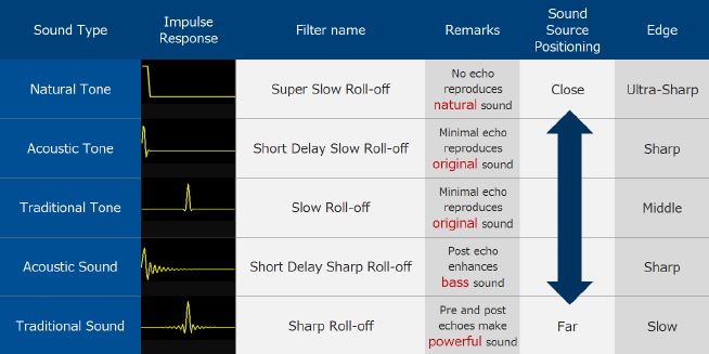
Native DSD Support
Supports 2.8MHz (64fs), 5.6MHz (126fs) and 11.2MHz (256fs) DSD
According to AKM, the volume control module and the delta-sigma modulator can be bypassed for DSD resulting in “direct” DSD rendering. The AK4490 contains an integrated low-pass filter specifically for DSD data. The ultimate specified performance for SACD (as described in the Scarlet Book) can be easily realized with a simple external analog filter.
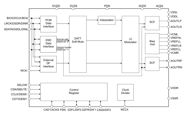
Notice the bypass path for DSD Data. The DSD data is received by the DSD interface and sent directly to the “SCF” (Switched Capacitor Filter) block. DSD filter can be selected at 50KHz, 100KHz or 150KHz cut-off.
Other Comparative Features
Resolution32 bit32 bit32 bit24 bit24 bit
| Parameter | AK4490EQ | ES9018 | ES9018K2M | WM8741 | PCM1794 |
| DR (Mono) | 123 dB | 135 dB | 127 dB | 128 dB | 132 dB |
| THD | -112 dB | -120 dB | -120 dB | -100 dB | -108 dB |
| Max SR | 768KHz | 384KHz | 384KHz | 192KHz | 192KHz |
| Output Mode | Voltage | V or I (best) | V or I (best) | Voltage | Current |
| Resolution | 32 bit | 32 bit | 32 bit | 24 bit | 24 bit |
| DSD Mode | DSD Direct and DSD to PCM | DSD to PCM | DSD to PCM | DSD Direct and DSD to PCM |
Just like the WM8741, the AK4490 supports “direct DSD” processing bypassing the volume control and delta-sigma modulator. And like the WM8741, there is no automatic switching between PCM and DSD.
I2S and DSD shared lines
In order to facilitate the playing of both PCM and DSD content, it is desirable to have the same lines transmit PCM and DSD data. We find that in the AK4490, the I2S and DSD signals are shared. Here is a post I write earlier concerning shared I2S/DSD signal lines: [link]
The table below shows compatible DACs (DACs that share that use the same lines for DSD and PCM) and interfaces showing how the DSD pins are mapped to the PCM/I2S pins:
| I2S Pins |
ESS9018 [link] |
PCM1795 [link] |
AK4399 [link] |
Amanero [link] |
SDTrans [link] |
XMOS Ref [link] |
| BCLK | DSD Clock | DSD Clock | DSD Clock | DSD Clock | DSD Clock | DSD Clock |
| LRCLK | DATA Left | DATA Right | DATA Right | DATA Left | DATA Left | DATA Left |
| DATA | DATA Right | Data Left | Data Left | Data Right | DATA Right | DATA Right |
The AK4490 DAC follows the mapping of the AK4399 which switches channels with the “conventional” channel mapping of USB interfaces. Likely it was the USB interface designers that took notice of the ESS9018 DAC and conformed the channel mapping to that chip.
Fortunately, there is channel remapping in at least the Amanero interface and there is channel remapping in the DAC itself as specified in the following table of the data sheet:

MONO=0, SELLR=1 says:
- Right channel input is mapped to Left channel output
- Left channel input is mapped to Right channel output
DIYINHK IMPLEMENTATION
I Just received diyinhk’s implementation of AKM’s new flagship DAC, the AKM AK4490EQ [link]. This is the first available diy board in the market (that I know of):

POWER SUPPLY LINES
The Diyinhk implementation follows (mostly) the AKM evaluation board and data sheet [link] but maximizes performance whenever possible (like in the selection of capacitor type and value). The board is powered by: 5V line, 3.3V line and +/- 12V line (for the output opamp).

The general layout of the power traces, decoupling capacitors and ground planes also follows the data sheet:
Grounding and Power Supply Decoupling:
To minimize coupling by digital noise, decoupling capacitors should be connected to AVDD and DVDD respectively. VREFHL/R and VDDL/R are supplied from analog supply in system, and AVDD and DVDD are supplied from digital supply in system. Power lines of VREFHL/R and VDDL/R should be distributed separately from the point with low impedance of regulator etc. AVSS, DVSS, VSSL and VSSR must be connected to the same analog ground plane. Decoupling capacitors for high frequency should be placed as near as possible to the supply pin.
Analog 5V supply lines (can operate up to 7.2V according to spec)
The 5V supply connects to VDD (5V Analog supply input) and Reference Voltage High (VREFH) -as recommended in the data sheet.
The differential voltage between VREFH-L/R and VREFL-L/R sets the analog output range. The VREFH-L/R pin is normally connected to VDD (analog 5V supply), and the VREFL-L/R pin is normally connected to VSS1/2/3 (analog ground). VREFH-L/R and VREFL-L/R should be connected with a 0.1µF ceramic capacitor as near as possible to the pin to eliminate the effects of high frequency noise…All signals, especially clocks, should be kept away from the VREFH-L/R and VREFL-L/R pins in order to avoid unwanted noise coupling into the AK4490.
In addition, according to the eval board manual, a large value capacitor between VREFH-L/R (Analog 5v) and VREFL-L/R (GND) improves the THD performance in accordance to the following graph:

The Diyinhk board is implemented with 2200 uF capacitors, achieving the best THD numbers. (The larger capacitor holds the reverence voltage stable -perhaps an even larger capacitor would further improve the low frequency THD numbers).
There is an option to use separate supplies for right and left VREF and VDD. This also follows the scheme implemented in the official evaluation board where the left VREF is separately powered from the right VREF.

Further, the AKM literature states:
Special designs techniques for sound quality are applied to each blocks for achieving balanced, smooth and powerful signal flow. In addition to L/R perfectly symmetrical layout, more than 5x trace width is used for signal line compared existing products, supplying rich current to analog signal output blocks. To achieve low impedance, two analog power supply pins and two signal reference pins are assigned for each channel, allowing the system to utilize thick PCB trace pattern giving low impedance sources.
The board takes advantage of this feature to use thicker lines for VREF and VDD
All 0.1 uF decoupling ceramic capacitors are C0G

The official evaluation board has a provision to separate the VREF from the Analog 5V VDD which is not implemented in this board. However, it is easy to mod and use separate supplies for VREF and Analog 5V VDD.
The evaluation board implements VREF with the following circuit:

3.3 V Supply Line (Analog 3.3V and Digital 3.3V)
There is a 3.3V analog supply pin and a 3.3V digital supply pin in the chip. The default implementation of the diyinhk board uses the same supply line but filters them with a ferrite bead. By removing the ferrite bead, the user can use separate supplies for the analog and digital 3.3V.

In the evaluation board, AVDD and DVDD are powered by separate regulators:


GROUND PLANE
The ground planes follows the recommended separation between analog and digital sides (along pins 17-18 and 45-46)


SOFTWARE INTERFACE
The older device, the AK4399 supported a 3-wire serial interface. This seemed a not too widely supported protocol (it was not SPI and could not find a similar protocol in Arduino libraries , but one could code the protocol “by hand” as it was just a serial protocol -never tried it though)
Fortunately the new DAC supports I2C protocol (and maintains support for the original 3-wire serial interface found in older DACs). This greatly facilitating the interface to a microcontroller such as Arduino because of their built-in support for more standard protocols such as I2C and SPI.
The advantage of using the S/W interface is that it supports features such as volume control and DSD which are not available through the H/W interface.
The following table summarizes these features that are available in H/W interface (parallel interface -by pulling hardware pins up or down) and S/W interface (serial interface -microcontroller control).

Not indicated in the table is the “super slow roll-off” filter which is enabled by a register setting in s/w mode.
REGISTER DEFINITION SUMMARY
(Updated with information from AKM support engineer)
Here I summarize the register settings and the different functions that can be programmed. I also attempt to do some “translating” of AKM’s vocabulary to more “traditional” vocabulary.
I was able to communicate with AKM to clarify the functionality of certain sections.
Register address: 00 (Control 1)
 7 6 5 4 3 2 1 0
|_|_|_|_|_|_|_|x| Reset chip without initializing registers
|_|_|_|_|x|x|x|_| Interface mode: 16bit, 24bit, 32bit, I2S, LJ... (1)
|_|_|x|_|_|_|_|_| External digital filter clock: 768KHz/384KHz
|_|x|_|_|_|_|_|_| Enable/disable external digital filter mode
|x|_|_|_|_|_|_|_| Master Clock frequency Setting: auto/manual (2)(3)

NOTES:
(1)- The only requirement for bitclock is >= 2x bit depth. Bitclock could be
32fs, 48fs or 64fs. Not limited to always be 64fs as in ESS DACs
(2)- Auto: detects master clock frequency and sampling frequency (44.1KHz,
96KHz, ...) automatically; sets oversampling rate (1x, 2x, 4x...) according to
input MCKL (this is kind of obvious).
Note: AKM calls sample rate "sampling speed" and assigns names to typical
sample rates: 44-48KHz="normal", 88-96KHz="double", 175-192KHz="quad"...
(3)- Manual: manually set the sampling rate (44.1KHz, 96KHz...) Use reg 01 and
reg 05 for sampling rate setting. This means, in its simplest form, manually
matching the sampling rate to the incoming data sample rate to use the highest
oversampling rate allowed by the system and thus obtain best noise performance.
This feature can also be used to select a different sampling rate (typically a
lower oversampling rate); for example, if selecting "normal" for 44.1KHz allows
8x oversampling (512fs), selecting "double" results in 4x oversampling (256fs).
This allows for experimentation with different oversampling rates and can be
used to tailor the sound for those inclined to lower oversampling or even no
oversampling. The use of lower oversampling results in higher noise for these
kind of DACs. AKM indicates in the datasheet that using a lower oversampling
rate (512fs to 256fs) results in a decrease of S/N of 3dB.

Register address: 01 (Control 2)
 7 6 5 4 3 2 1 0
|_|_|_|_|_|_|_|x| Mute/unmute
|_|_|_|_|_|x|x|_| De-emphasis: Off, 32KHz, 44.1KHz, 48KHz
|_|_|_|x|x|_|_|_| Manual setting of sampling speed: "normal", "double"... (1)
|_|_|x|_|_|_|_|_| Short Delay/Traditional filter (Minimum/Linear phase)
|_|x|_|_|_|_|_|_| Zero data detect mode: Separate channels or ANDed channels
|x|_|_|_|_|_|_|_| Zero data detect ON/OFF

NOTES:
(1)- Manual sampling speed setting uses 3 bits. The third bit is in reg 05.
See notes on register 00 for additional info on manual settings

Register address: 02 (Control 3)
 7 6 5 4 3 2 1 0
|_|_|_|_|_|_|_|x| Filter cutoff slope: fast/slow
|_|_|_|_|_|_|x|_| MONO mode: left/right
|_|_|_|_|_|x|_|_| Invert output pin level on zero detect
|_|_|_|_|x|_|_|_| MONO/STEREO mode
|_|_|_|x|_|_|_|_| DSD Data on clock falling/rising edge
|_|x|_|_|_|_|_|_| DSD master clock frequency:512KHz/768KHz
|x|_|_|_|_|_|_|_| PCM/DSD mode

Register address: 03 (Left Channel Attenuation)
 7 6 5 4 3 2 1 0
|x|x|x|x|x|x|x|x| Attenuation (1)
NOTES:
(1)- 256 levels, 0.5 dB each. 00=mute; ff=max volume

Register address: 04 (Right Channel Attenuation)
 7 6 5 4 3 2 1 0
|x|x|x|x|x|x|x|x| Attenuation (1)
NOTES:
(1)- 256 levels, 0.5 dB each. 00= mute; ff= max volume

Register address: 05 (Control 4)
 7 6 5 4 3 2 1 0
|_|_|_|_|_|_|_|x| Super Slow filter on/off
|_|_|_|_|_|_|x|_| Bit 3 of the manual sampling speed setting (see reg 01)
|_|x|_|_|_|_|_|_| Left channel phase invert ON/OFF
|x|_|_|_|_|_|_|_| Right channel phase invert ON/OFF

Register address: 06 (control 5)
 7 6 5 4 3 2 1 0
|_|_|_|_|_|_|_|x| DSD bit 0 of sampling speed selection (bit 1 is in reg 9)(1)
|_|_|_|_|_|_|x|_| DSD Mode: Direct/Convert to PCM (2)
|_|_|_|_|x|_|_|_| DSD Automute release when Automute release is in "hold"
|_|_|_|x|_|_|_|_| Automute release: Auto/hold (3)
|_|_|x|_|_|_|_|_| Right Channel DSD flag when detecting full scale signal
|_|x|_|_|_|_|_|_| Left Channel DSD flag when detecting full scale signal
|x|_|_|_|_|_|_|_| DSD AutoMute: ON/OFF (4)

NOTES:
(1)- There is no facility for setting auto sample rate detection for DSD. The
use must detect the incoming DSD sample speed and match the sampling speed.
Will have to experiment to see what is the effect of sample speed mismatch.
(2)- In DSD direct mode, the volume control and delta-sigma modulator are
bypassed. In PCM mode, it converts to PCM and uses volume control block and
delta-sigma modulator. DSD direct with a combination of the internal filter
and simple output filter meets the filter specification of the SACD Scarlet
Book.
(3)- Automute condition disappears when data becomes under full scale
(4)- Automute condition is when data is full scale

Register address: 07 (Control 6)
 7 6 5 4 3 2 1 0
|_|_|_|_|_|_|_|x| Synchronize ON/OFF (1)

NOTES:
(1) Synchronizes multiple DACs when used together in the same system. Read
data sheet for more information.

Register address: 08 (Control 7)
 7 6 5 4 3 2 1 0
|_|_|_|_|_|_|x|x| Sound Quality Control Setting (1)

NOTES:
(1): Sound Control has 3 settings: "1", "2", "3". The AK4495 data sheet shows
additional settings "4" and "5". These setting refer to the 5 different filters
that are available in the DAC. They serve the same function as the filter
selection bits specified in the other registers. What is unclear is which
register takes precedence.

Register address: 09 (Control 8)
 7 6 5 4 3 2 1 0
|_|_|_|_|_|_|_|x| DSD bit 1 of sample speed selection (see also reg 5)
|_|_|_|_|_|_|x|_| DSD filter selection when in DSD direct mode

Latest Comments