$99 ES9018 DIY DAC BOARD
DIY INDEED…
Just received the board. Very good quality, some photos below… This is the V2 version of the board. This version came quickly after V1 and (to my surprise and delight) implemented many of the things I suggested in the diyaudio thread. That is pretty good response from the creator of this board. In this eBay website, he mentions that this design will keep on evolving, thus I would encourage anyone interested in this board or future iterations to provide feedback and suggestions at his diyaudio thread.
It is good to see another DIY version of this DAC especially at this low price. But this requires the most work. Keeping in mind that the chip alone would cost $60, the price of this DAC board is near cost. So if you are handy with soldering small components, this board should provide plenty of fun and audio satisfaction.


All the input lines are available (e.g.: not grounded) -this is an improvement from V1. The output is stereo, so it can be used as stereo or mono but not 8-channle. However, having all the inputs available, we can leverage the internal mux and auto-detection to switch between different inputs.

There are pads for U.FL connector for clock input on the other side of the board. This is also an improvement from V1

Pads seems fairly easy to solder. I believe it can accommodate a 1206 SMD capacitor or a 5 mm-leads radial capacitor. Footprint for any size oscillator including the Crystek CCHD-950/957

This gives you an idea on the dimensions of the solder pads:

BYPASS CAPACITORS
The first thing to figure out are the power bypass capacitors. The board has space for both SMD capacitors and through hole capacitors. One idea is to mount both of them (of different values) in order to improve filtering:
According to this application note from TI [link]
The most common values bypass capacitors are: 47 µF, 22 µF, 4.7 µF, 0.1 µF, and 0.001 µF. The higher value capacitors (47 µF and 4.7 µF) work well at relatively low frequency (low-frequency bypass). The 0.1 µF targets the middle frequency range, while the 0.001 µF or smaller capacitors handle higher frequencies (high frequency bypass). Choosing two or three capacitors with different capacitance ranges will effectively filter a wider noise bandwidth.
Seems using a 0.1 uF SMD capacitor with a radial 0.001 capacitor is an excellent idea…
(Update 1/4/13: more photos)
Front side of entire board. Since I probably got the first V2 board, the ADP 1.2 regulator was not soldered… The solder pads are all silver in color. The coloring is reflection of the surrounding, including the sky…

Back side of board

Input connections details (front and back)


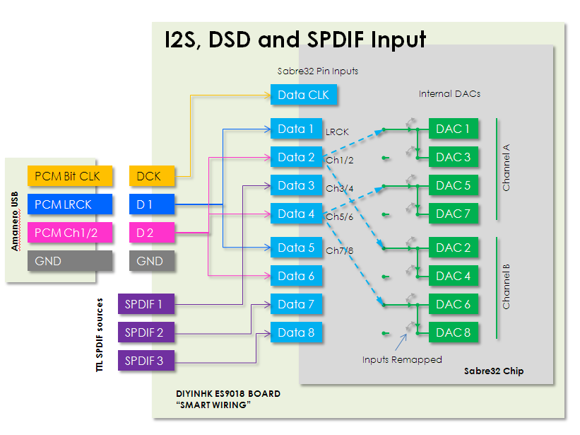
Notice that D5, D4, D3 and D2 are tied together for default stereo I2S operation and connected to the front “data” pad. In order to use the inputs separately, one needs to cut them.

(Update 1/4/13: Chip bypass)
I’ve traced the power supply bypass positions and labeled them. There are 8 bypass locations for the most important supply the 3.3V analog (AVCC), 3 bypass locations for the 1.2V and 2 bypass locations for the 3.3V digital supply. I am not sure if the 1.2V locations would just require a 10 uF bypass (which are indicated in the ESS available documents) I think having a 0.1 uF SMD together with a 10 uF electrolytic on the other side is a better bypass.
Every AVCC pin has its bypass capacitor, but not every 3.3V Digital and 1.2V has its own bypass capacitor. Doesn’t seem to be enough space (or required?), but the seller did put the bypass where it most counts, the analog AVCC

(Update 1/5/13: Reset, power supplies)

Two external supplies are to be provided: a supply for the analog section and a supply for the digital section. The 3rd power supply is the 1.2V and it is provided by a local regulator that must be installed (I believe the current boards already come with this regulator installed).
The 3.3V analog or AVCC supply is the most critical. Preferably, choose a low noise shunt-type. I have yet to decide what to use. I may built up some of the Placid V1 boards I have.
For the 3.3V digital, I plan to use the TPS7A47 Eval Board.

(Update II 1/5/13: Differential Vout, chip address, AVCC/2 offset, I/V)
I am a fan of using the Sabre32 DAC in differential voltage out mode. I have been using the Buffalo II DAC this way since day one and still do not have the motivation to add an I/V stage :-). There has been comparison of this DAC in voltage mode against other DACs and I’ve documented some here: [link].
BTW, if you are concerned that only an optimally routed fabricated and designed board can produce good sound, you should take a look at what Mr Abraxalito is up to: [link] 🙂
I plan on using this DAC in voltage mode also, at least from the beginning. You can take the raw differential outputs as shown below and take the GND from any nearby GND pads

The chip address is already set at “o” -connected to GND. If you are using the board in stereo mode, there is no need to do anything here. For mono operation you would have to cut the trace for one of the boards and connect the address pin to VDD (set to “1”)

The 2 10K resistors establish the AVCC/2 offset voltage that is used by the I/V stage

The I/V output stage is an implementation of the circuit in the 2-channel eval board [link]
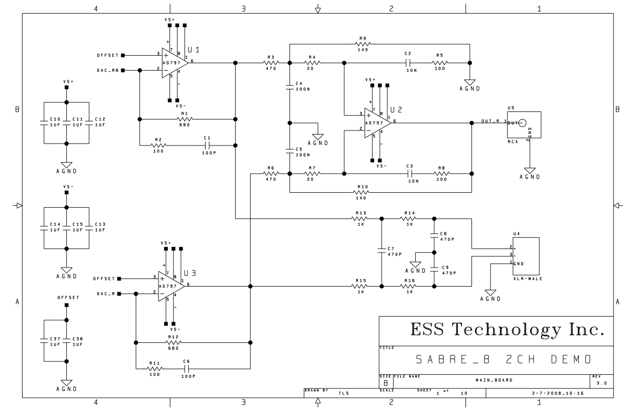

The schematic calls for 1 uF bypass for the power supply lines and voltage offset lines. Probably a good idea to use a 0.1 uF SMD bypass together with a 10 uF electrolytic bypass.

(Update 01/6/13: Correction on reset circuitry)
Seller sent me a message indicating that the reset circuit must be populated or else the DAC will be unstable. This makes sense as the pin is floating if none of the components are installed. I’ve corrected the instructions above.
(Update II 01/06/13: Buffered differential output)
The board only implements output pads only for single ended output, but since this is diy, you can take the output basically anywhere you wish.
The buffered differential outputs can be taken off the outputs of the opamps. By implementing the opamp I/V converter, you “force” the DAC into current mode allowing for better THD.

And then add the low pass filter specified in the ESS documentation
(Update 01/08/13: More on using the DAC in voltage mode)
Using the DAC in voltage mode means not needing to populate the opamps. According to the designer of the DAC:
… The current mode is simply when the current going in and out the pin of the chip is being sensed. This mode has the benefit of cancelling 2nd and 3rd harmonics of some of the internal analog circuitry.
The “voltage mode” is when the pin of the chip has a voltage that is being sensed. While this has the 2nd and 3rd harmonics (at the -100dB level or so), some people have even claimed this mode is more “tube-like”. It is all personal preference. [link]
(Update II 01/08/12: Using Hifiduino s/w and Arduino controller)
The current version of the Hifiduino s/w [link] supports the following configurations for the board:
1- The board in its default configuration which is I2S and SPDIF in Data 7 and Data 8 simultaneously

2- Inputs modified to match the input wiring for Buffalo II: will support both I2S and DSD with an input board such as Amanero and also SDPIF on Data 1 if not using I2S

3- Inputs modified to support “smart” wiring: will support both I2S and DSD with an input board such as Amanero and also SDPIF on Data 1, Data 7 and Data 8 (SPDIF in TTL levels – 3.3v)
Notes:
- SPDIF inputs are TTL level. You cannot just take the spdif output from a consumer device such as a DVD player.
- Unused inputs should be grounded
- All inputs should have a termination resistor
Continue reading here: Part I: [link]

yeah but having the smaller one leaded is the wrong way around.
Hi qusp, I read somewhere that because of the inductance of the leads, a 0.1 uF capacitor may oscillate at 80 MHz, That is why I think using SMD for the 0.1 uF is a good idea…
well SMD for both would be better, it just doesnt make a lot of sense to me to have the much smaller cap have some inductance that means its resistive in the VHF you are trying to bypass.
Looks very interresting. Do you have a link to where you got the board?
eBay: http://www.ebay.com/itm/ES9018-32bit-Audio-DAC-PCB-kit-/330849729368?pt=US_Amplifier_Parts_Components&hash=item4d082e3b58
or do a “ES9018” search in eBay
Nice. In this configuration it would make more sense using ESS 9012 chip, since output is 2 channel only.
Probably, although I have not seen many implementations using ES9012. Perhaps the 9018 is more plentiful and easier to get.
And both chips cost the same: $55 http://www.shawelectronics.com/samples.html and $65 here: http://ecommerce.ismosys.com/ordering/product_info.php?manufacturers_id=34&products_id=479
Very interesting kit, I checked the seller’s ebay site and looks like it has 6 x 8 pin DIP so I guess it has both I/V plus BAL->SE and LPF. Did you get a building manual or any indication as to which parts to use in those positions? ESS recommends the AD797 on their data sheet but I read it is quite a “delicate” amp oscillation wise.
No documentation. According to diyinhk, it is based on ESS reference implementation.
However, I hope we can all share information to determine the best components to use. diyinhk has a thread in diyaudio where we can provide feedback for the next version of the board…
I just ordered one. Thank you for the tip.
Looking forward to seeing more of what you can do with it. I take it that you will test this with Ian`s Fifo solution?
That is the “obvious solution” since it has no on-board clock 🙂
You could also try driving it in sync mode from the Amanero, it shouldn’t be too bad up to 88.2/96 and IMHO would make more sense in a tight budget project.
I’m looking at your (gorgeous) photos and it seems to me that D5 through D2 are connected to each other (and to ground?). If that is indeed so, it would make those inputs useless.. Unless one could separate them, perhaps by cutting through the traces?
You are right. Didn’t notice that. Yeap, just get a knife and cut the trace…
Indeed. Need to cut that trace if the mux is to be used.
Could you take some images of the entire board top and bottom?
got any pics of under the board, this is actually where most of the action is going on with ESS and where you would see if its quality or not, i’ve not seen any pics of underneath yet anywhere. also it uses the old 1 ground for all digital inputs?…. not ideal.
1 shared ground I mean? thats what it looks like
Yes, contrary to popular belief, there is a single ground plane. diyinhk took the recommendations of ESS to heart: This is from one of the documents in their website:
“Proper PCB layout for the Sabre DAC is vital to the circuit’s performance. Time spent achieving optimum component placement provides a good foundation to make the routing task provide the best performing circuit within the real estate provided. Every design will have different requirements, PCB stackup, via size, PCB size, component sizes, etc. ESS has experimented with DAC evaluation PCBs ground planes to determine any benefit of split plane grounds for analog and digital ground. It is our finding and recommendation to use only one ground plane for both digital and analog grounds as it simplifies layout and provides no performance degradation. The most important for DAC performance is the ground plane, it should be as solid as possible with as few traces routed through the ground plane as possible. Any traces that are routed through the ground plane and block the “line of sight” from the DAC output to the opamp output stage significantly degrades the output THD”
I too was looking at a separation of digital and analog grounds… Will put up some pics when I get a chance…
thats not what I meant, I mean the header at the top has only a single ground return connection for ALL of the digital inputs to share; this is bad design that is unfortunately all too common.
Segmented but shared ground plane is fine, the ackodac does this too, but it has slots cut (not traces crossing) to segregate the circulating ground currents and help encourage the loop area for each supply pin/channel to be confined to its own section. and this is to an extent mirrored on the top side with the sectioned power planes, so the power/return loop area can take its natural course. they all join at a single small point under the dac, while the plane is completely solid but for that. this is why I wanted to see under the board.
funny you quote that section, I was going to link it, the line of sight is not unbroken for the analogue outputs on this board, there is a via to skip under the other polarity directly on the output pins. strange clock trace routing too, too many traces crossing over or under components etc.
he hasnt got a keepout under the pattern for the clock u.fl connector as there should be either, so there is ground fill under the socket.
some of this is nit-picking, some of the problems are significant. cheap entry into playing with ESS yes, but I wonder how much it will all add up to as an individual buying components plus shipping
Hi qusp, thanks for the explanation. I’ll have to think though it to visualize what you mean… What I like about this guy is that he is quick to implement changes.
that is, a return current likes to flow underneath the associated power/signal current
no termination on the digital lines either….
Are they any plans to update the hifiduino code to work with this $99 board? Thanks!
The code should work as is. Best is to wire the inputs like Buffalo II.
Hello, is HIFIDUINO code compatible with this board? I have ordered the board and would like to use the HIFIDUINO code.
Fully compatible. Just wire the inputs like Buffalo II. Here is what the latest version supports: https://hifiduino.wordpress.com/2012/11/28/new-version-of-hifiduino-code-for-sabre32-dac/
Thanks for the comments and updating the section with pictures.
Hello, does ES9018 works in hardware mode with I2S?
I connect XMOS module, didnt populate op-ams, SAW 75MHz, but no lock state in LED.
i using SAW 75MHz clock
Yes, it does work in H/W mode. DAC locks to bitclock.
Hi, i have check all voltages, connections, but still no lock (luck:)).
Does need to use software mode for SAW 75Mhz? Which is default freq.?
Should work in h/w mode with 75 MHz. There is no “default” frequency.
Hi,
thanks.
Finally DAC is working :)) I had bad connection on I2S lines.
Good to hear. “Smart wiring” requires that the inputs (D0-D7) are not connected to each other. The code works with the Amanero board and supports both I2S and DSD.
Forgive my ignorance [I know little about electronic engineering] but can you have 3 inputs to the DAC, S/Pdif, USB, Toslink? I’ve a home-brew amplifier project and I’m looking for a solution to take these 3 inputs to a very good DIY DAC.
What does it mean the spdif is TTL,what does it take to drive it from a “regular” Spdif output?
It means the DAC expects 3.3v. The consumer (regular) SPDIF is about 1 v.
How do I make the DAC accept regular Spdif?
Здравствуйте! Подскажите где реально взять в ближайшие дни ссуду?
battlefield play4free funds generator
poker online
suga kuk